Using plated surface for recording media without polishing

a technology of plated surface and recording media, which is applied in the direction of electrolytic organic material coating, superimposed coating process, instruments, etc., can solve the problems of adversely affecting the writing of information to the magnetic disk, achieve high degree of surface smoothness, facilitate the manufacture of magnetic recording media, and improve the overall process throughput

Inactive Publication Date: 2002-06-13
SEAGATE TECH LLC
View PDF0 Cites 1 Cited by
  • Summary
  • Abstract
  • Description
  • Claims
  • Application Information

AI Technical Summary

Benefits of technology

0016] The present invention advantageously achieves formation of composite nickel coatings on non-magnetic substrates having a surface roughness (Ra) less than about 10 .ANG.. The achievement of such ultra-smooth as-deposited composite nickel coatings yields several technological advantages. For example, after the composite nickel coating is formed on the non-magnetic substrate, the high degree of surface smoothness eliminates the need for a subsequent polishing step. As such, the composite coated substrate may be used directly for a media deposition process, improving the overall process throughput for the manufacture of magnetic recording media. The composite nickel coatings having an as-deposited ultra-smooth surface enables and facilitates the manufacture of magnetic recording medium having high areal recording density, with reduced flying heights for the head.
0017] The present invention stems from the discovery that the deposition of a sputtered nickel layer on a substrate prior to the deposition of an electrolessly plated nickel layer thereover provides a composite nickel coating having a surface roughness that is significantly smoother than that of traditionally deposited electroless nickel layers. Furthermore, as illustrated in FIG. 1, the degree of surface smoothness appears to be enhanced as the thickness of the underlying sputtered nickel layer is increased.

Problems solved by technology

The absence of defects such as, for example, pits is especially important, since pits may adversely affect the writing of information to the magnetic disks.

Method used


Image

  • Using plated surface for recording media without polishing
  • Using plated surface for recording media without polishing
  • Using plated surface for recording media without polishing

Examples


example 2

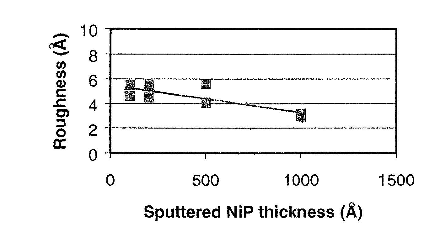
[0034] A nickel phosphorus (NiP) composite coating was prepared. The NiP composite coating was prepared by sputtering a nickel-phosphorus (NiP) layer on a TiW coated Ohara TS-10 SXSP glass-ceramic disk. The NiP was sputtered from a NiP target comprising about 25 atomic % nickel. The sputter deposited NiP layer had a thickness of about 500 .ANG.. A 1 micron thick nickel phosphorus (NiP) layer was electrolessly deposited over the sputter deposited NiP layer. The NiP layer was electrolessly plated from an Enthone 6450 Ni plating bath.

[0035] The surface roughness of the as-deposited composite nickel layer was measured using AFM (Atomic Field Microscopy). A 10 micron.times.10 micron scan of the composite nickel coating indicated a surface roughness (Ra) of about 5.6 .ANG..

example 3

[0036] A nickel phosphorus (NiP) composite coating was prepared. The NiP composite coating was prepared by sputtering a nickel-phosphorus (NiP) layer on a TiW coated Ohara TS-10 SXSP glass-ceramic disk. The NiP was sputtered from a NiP target comprising about 25 atomic % nickel. The sputter deposited NiP layer had a thickness of about 200 .ANG.. A 1 micron thick nickel phosphorus (NiP) layer was electrolessly deposited over the sputter deposited NiP layer. The NiP layer was electrolessly plated from an Enthone 6450 Ni plating bath.

[0037] The surface roughness of the as-deposited composite nickel layer was measured using AFM (Atomic Field Microscopy). A 10 micron.times.10 micron scan of the composite nickel coating indicated a surface roughness (Ra) of about 5.5 .ANG..

example 4

[0038] A nickel phosphorus (NiP) composite coating was prepared. The NiP composite coating was prepared by sputtering a nickel-phosphorus (NiP) layer on a TiW coated Ohara TS-10 SXSP glass-ceramic disk. The NiP was sputtered from a NiP target comprising about 25 atomic % nickel. The sputter deposited NiP layer had a thickness of about 100 .ANG.. A 1 micron thick nickel phosphorus (NiP) layer was electrolessly deposited over the sputter deposited NiP layer. The NiP layer was electrolessly plated from an Enthone 6450 Ni plating bath.

[0039] The surface roughness of the as-deposited composite nickel layer was measured using AFM (Atomic Field Microscopy). A 10 micron.times.10 micron scan of the composite nickel coating indicated a surface roughness (Ra) of about 5.5 .ANG..

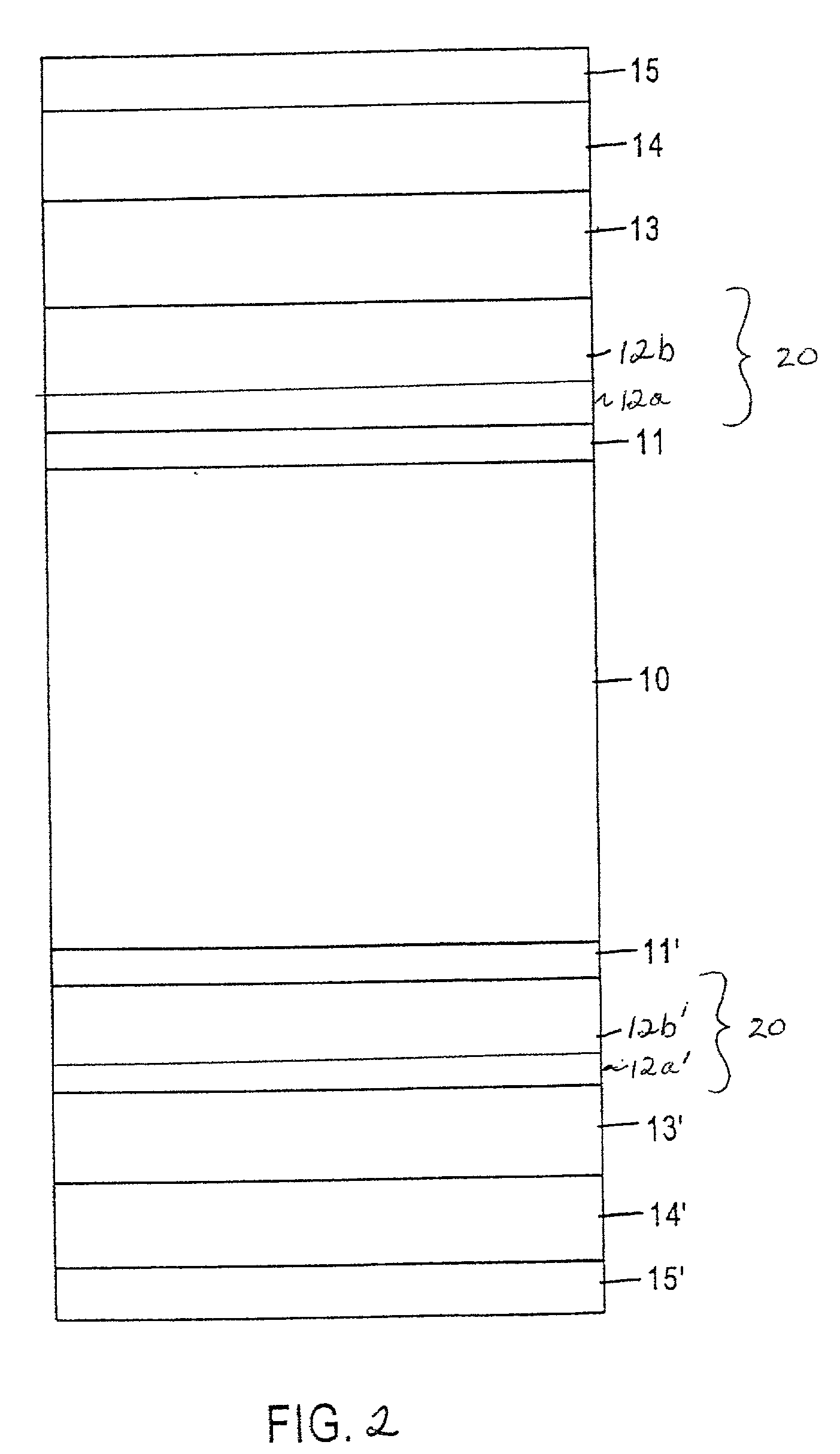
[0040] Referring again to FIG. 2, after the composite nickel coating 20 is formed on the substrate 10 the magnetic medium is deposited thereon. The magnetic medium typically includes an underlayer 13, 13', such as chrom...


PUM

PropertyMeasurementUnit
thicknessaaaaaaaaaa
thicknessaaaaaaaaaa
Raaaaaaaaaaa

Abstract

Ultra smooth as-deposited composite nickel coatings for use in an information storage system are provided. The composite nickel coatings include an electrolessly deposited nickel layer formed on a sputter deposited nickel layer. The composite nickel coatings have an as-deposited surface roughness of less than about 10 Å. Embodiments include formation of the composite nickel coating on a disk, followed by deposition of an underlayer and magnetic layer thereon to form a magnetic recording medium.

Description

[0001] This application claims priority benefit of U.S. Provisional Patent Application Serial No. 60 / 232,897 filed Sep. 15, 2000, entitled USING PLATED SURFACE FOR RECORDING MEDIA WITHOUT POLISHING in the name of Connie C. Liu, Linda L. Zhong, Ian J. Beresford, Lin Huang, Joseph Leigh, and David E. Brown, which is herein incorporated by reference in its entirety.THE INVENTION[0002] The present invention relates to nickel-coated substrates. The invention has particular applicability to the manufacture of magnetic recording media.[0003] Nickel (Ni) plating, particularly electroless Ni platings or deposits, enjoys technological applicability in various industries, such as the electronic, oil and gas, aerospace, machinery, automobile and magnetic recording media industries. For example, in magnetic recording media applications, a magnetic disc comprising a non-magnetic substrate such as aluminum (Al) or an aluminum alloy may be coated with an amorphous nickel deposit.[0004] Magnetic dis...

Claims


Application Information

Patent Timeline
Patent Type & Authority Applications(United States)
IPC IPC(8): G11B5/73G11B5/82G11B5/84
CPCG11B5/7325G11B5/8404G11B5/82G11B5/7368G11B5/73913
Inventor LIU, CONNIE C.ZHONG, LINDA L.BERESFORD, IAN J.HUANG, LINLEIGH, JOSEPHBROWN, DAVID E.
Owner SEAGATE TECH LLC
Why Eureka
Try Eureka