

Lithography method for forming semiconductor devices on a wafer and apparatus
a technology of lithography and semiconductor devices, applied in photomechanical devices, instruments, optics, etc., can solve the problems of increasing the requirements for overlay and critical dimensions (cds), requiring more precision, and the inability to measur
- Summary
- Abstract
- Description
- Claims
- Application Information
AI Technical Summary
Benefits of technology
Problems solved by technology
Method used
Image

Examples
Embodiment Construction
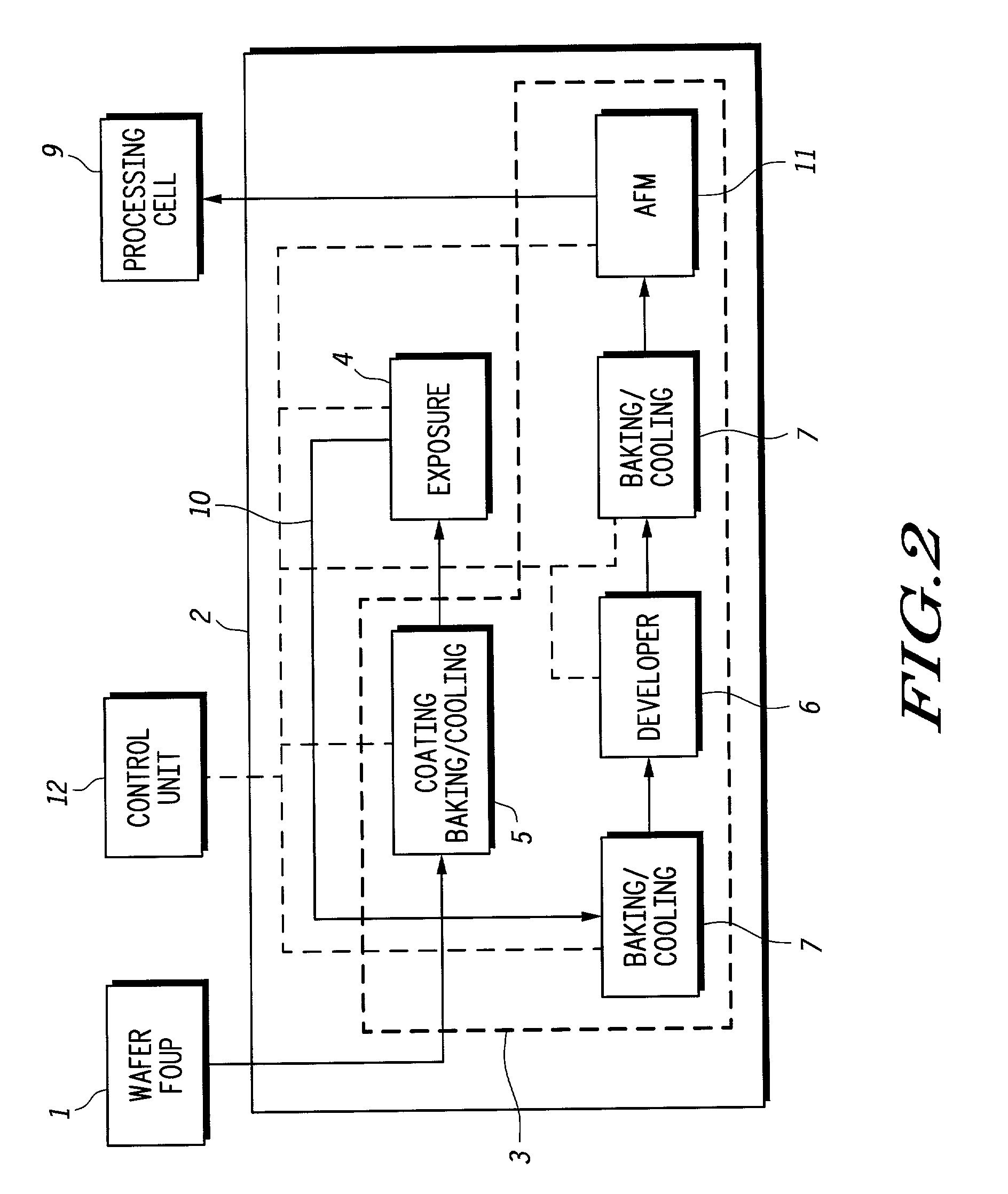
[0009] According to the present invention conventional optical overlay metrology is replaced with a metrology technique that is not currently used for lithography measurements. This technique can also be applied to measure critical dimensions (CDs) of the sub-micrometer features that are being printed on a wafer in the same module. The technique used by this invention is atomic force microscopy (AFM). The microscopy module is located within the lithography cell. This tool provides for atomic scale alignment and feature measurement accuracy. One advantage of the proposed technique is that this system is not prone to the errors associated with optical metrology.
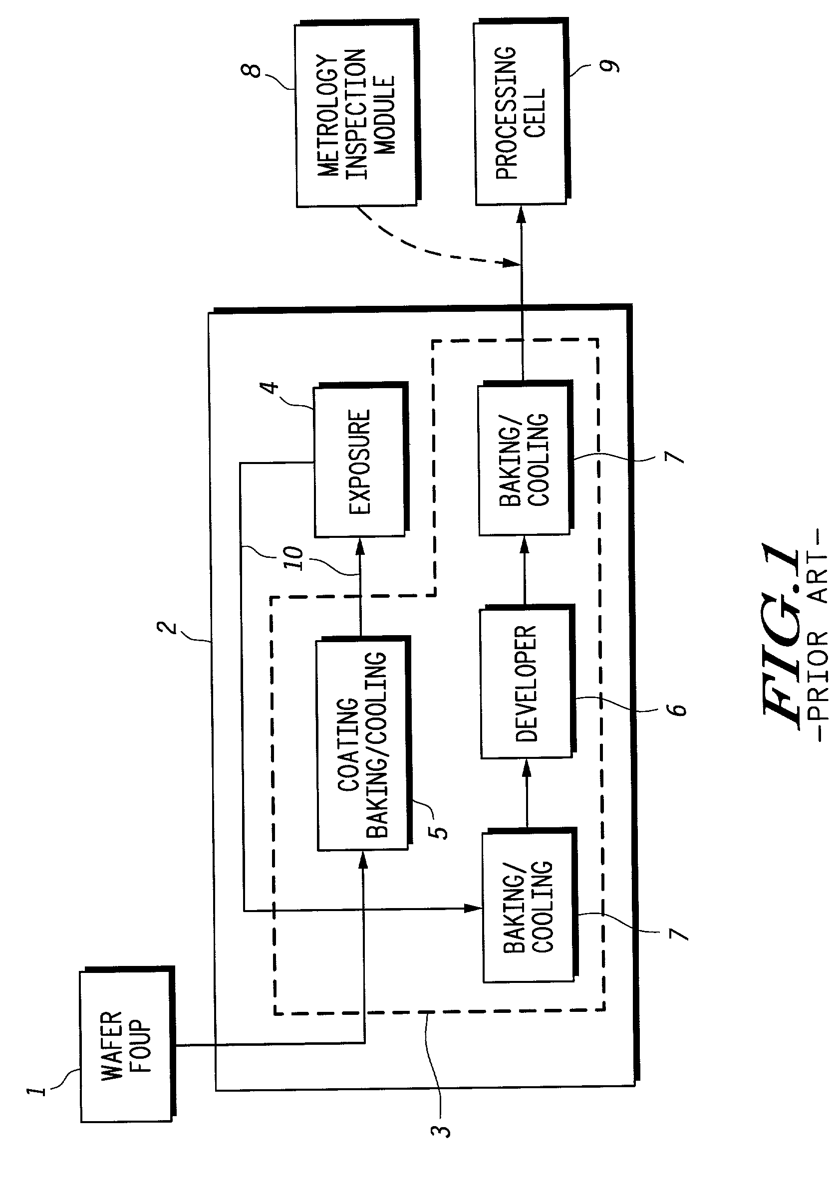
[0010] Referring to FIG. 1, there is shown a prior art design of a lithography cell and relevant adjacent tools. The wafers to be processed are carried in a Front Opening Unified Pod (FOUP) 1 which contains e.g. 25 wafers of 300 mm diameter. The wafer FOUP 1 enters into a lithography cell 2 which comprises as main components a ...
PUM
 Abstract
Description
Claims
Application Information