

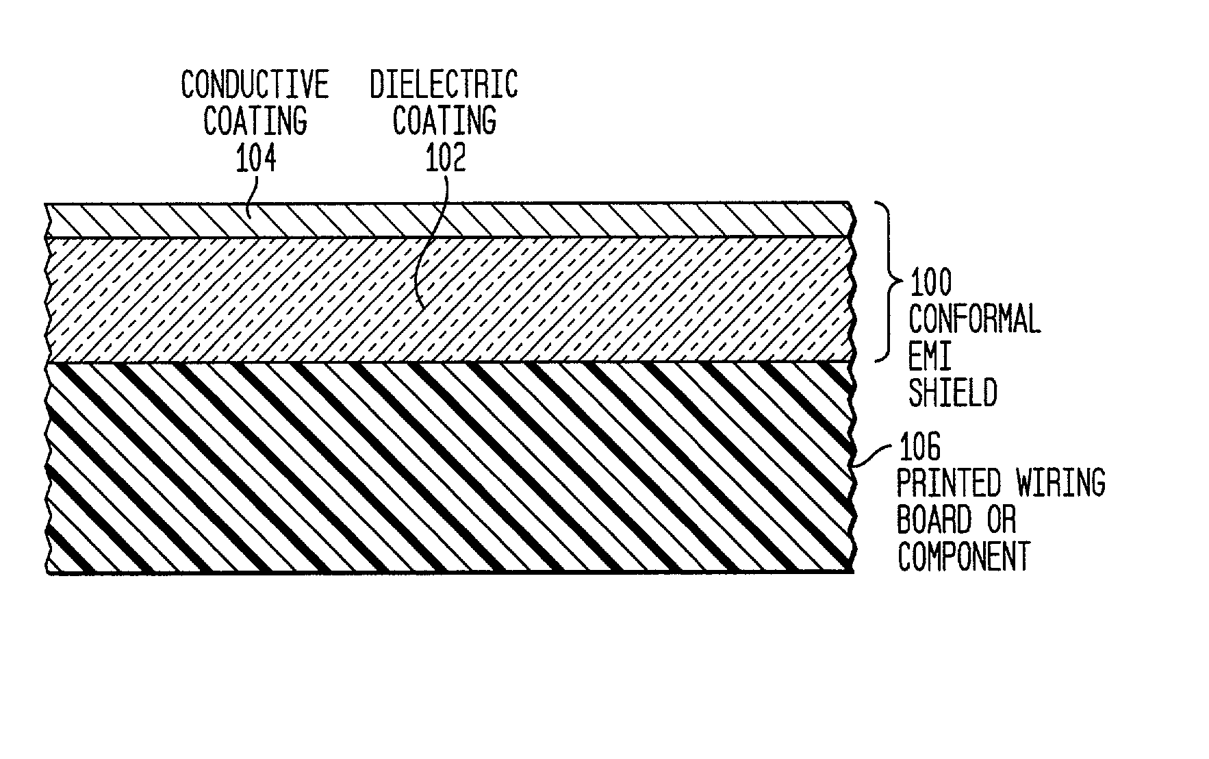
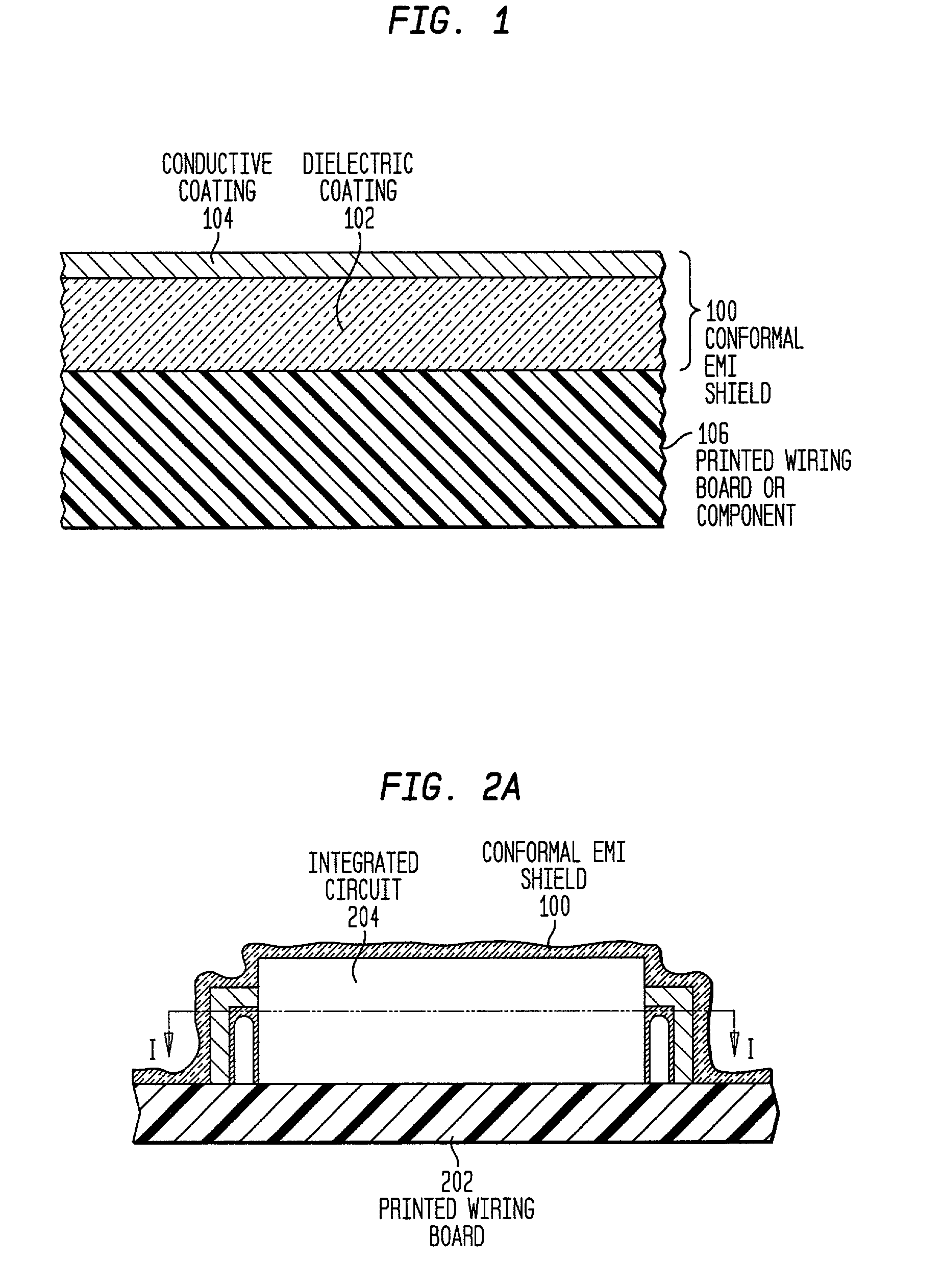
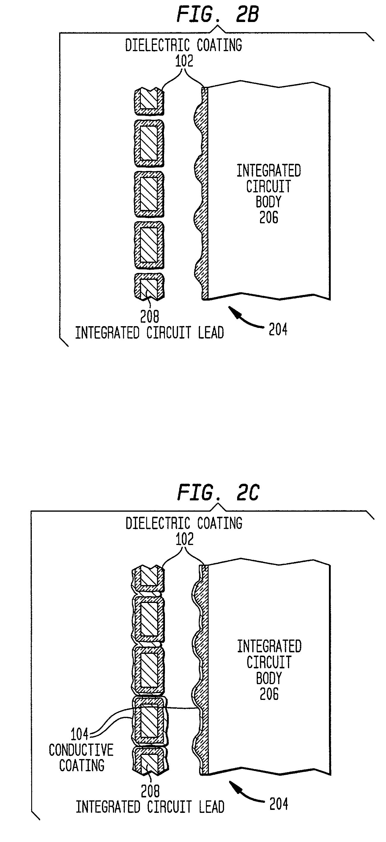
Board-level conformal EMI shield having an electrically-conductive polymer coating over a thermally-conductive dielectric coating
a technology of dielectric coating and conformal emi shield, which is applied in the direction of non-metallic protective coating application, cross-talk/noise/interference reduction, transportation and packaging, etc., can solve the problems of lack of shielding effectiveness, limited shielding success, and problematic emi, so as to reduce the cost and weight of sheet metal, promote heat distribution, and eliminate the effect of conventional metallic emi boxes
- Summary
- Abstract
- Description
- Claims
- Application Information
AI Technical Summary
Benefits of technology
Problems solved by technology
Method used
Image

Examples
example 2
2 Boron Nitride & Urethane Dispersion 1500 Thermal loading material 1400: 10%-80% BN, 0.1-10 micron powder Binder 1504: 90%-20% Urethane Base Liquid 1506: water or organic solvent Curing: UV and / or thermally cured
[0083] The binder 1504 and base liquid 1506 can be provided in the above-noted urethane intermediate dispersions. In accordance with the present invention, such intermediate dispersions are doped with the specified thermal loading material 1400 to form one embodiment of thermally conductive dielectric dispersion 1500.
3 Example 3: Aluminum Oxide & Acrylic Dispersion 1500 Thermal loading material 1400: 10%-80% Al.sub.2O.sub.3, 100 mesh, 99% corundum, alpha-phase Binder 1504: 90%-20% Acrylic Base Liquid 1506: water or organic solvent Curing: UV or thermally cured
[0084] The binder 1504 and base liquid 1506 can be provided in the above-noted acrylic intermediate dispersions. In accordance with the present invention, such intermediate dispersions are doped with the specified the...
example 4
4 Aluminum Oxide & Urethane Dispersion 1500 Thermal loading material 1400: 10%-80% Al.sub.2O.sub.3, 100 mesh, 99% corundum, alpha-phase Binder 1504: 90%-20% Urethane Base Liquid 1506: water or organic solvent Curing: UV and / or thermally cured
[0085] The binder 1504 and base liquid 1506 can be provided in the above-noted urethane intermediate dispersions. In accordance with the present invention, such intermediate dispersions are doped with the specified thermal loading material 1400 to form one embodiment of thermally conductive dielectric dispersion 1500.
5 Example 5: Magnesium Oxide & Acrylic Dispersion 1500 Thermal loading material 1400: 10%-80% MgO, 150 mesh Binder 1504: 90%-20% Acrylic Base Liquid 1506: water or organic solvent Curing: UV or thermally cured
[0086] The binder 1504 and base liquid 1506 can be provided in the above-noted acrylic intermediate dispersions. In accordance with the present invention, such intermediate dispersions are doped with the specified thermal load...
PUM
| Property | Measurement | Unit |
|---|---|---|
| conductivity | aaaaa | aaaaa |
| dielectric constant | aaaaa | aaaaa |
| dielectric constant | aaaaa | aaaaa |
Abstract
Description
Claims
Application Information