Semiconductor memory device

a memory device and semiconductor technology, applied in semiconductor devices, digital storage, instruments, etc., can solve the problems of increasing chip cost, increasing manufacturing steps, and large chip siz

Inactive Publication Date: 2002-11-21
RENESAS ELECTRONICS CORP
View PDF0 Cites 46 Cited by
  • Summary
  • Abstract
  • Description
  • Claims
  • Application Information

AI Technical Summary

Problems solved by technology

Thus, problems that the number of manufacturing steps increases significantly and chip costs increases are caused.
Thus, when an SRAM is used as a main memory having a large memory capacity, the size of the chip becomes very large.
Accordingly, it is very difficult to ...

Method used


Image

  • Semiconductor memory device
  • Semiconductor memory device
  • Semiconductor memory device

Examples


third embodiment

[0227] FIG. 23 is a diagram schematically showing the configuration of a modification of the present invention. In FIG. 23, a bank A sense amplifier band SABA is arranged at one side, in the column direction, of a row block RBA, and a bank B sense amplifier SABB is arranged between row blocks RBA and RBB. Memory cells arranged at the crossing of a bit line pair BLPa and a sub word line SWLA in row block RBA are connected to a sense amplifier in bank A sense amplifier band SABA. On the other hand, in row block RBA, data in memory cells arranged corresponding to the crossing of a sub word line SWLB and a bit line pair BLPb are sensed and amplified by bank B sense amplifier band SABB.

[0228] A local control circuit 85 is provided to bank A sense amplifier band SABA, and a local control circuit 86 is provided to bank B sense amplifier band SABB. A latch bank designating signal BSLTA and a latch block selecting signal BSA specifying memory blocks sharing bank A sense amplifier band SABA a...

fourth embodiment

[0233] [Fourth Embodiment]

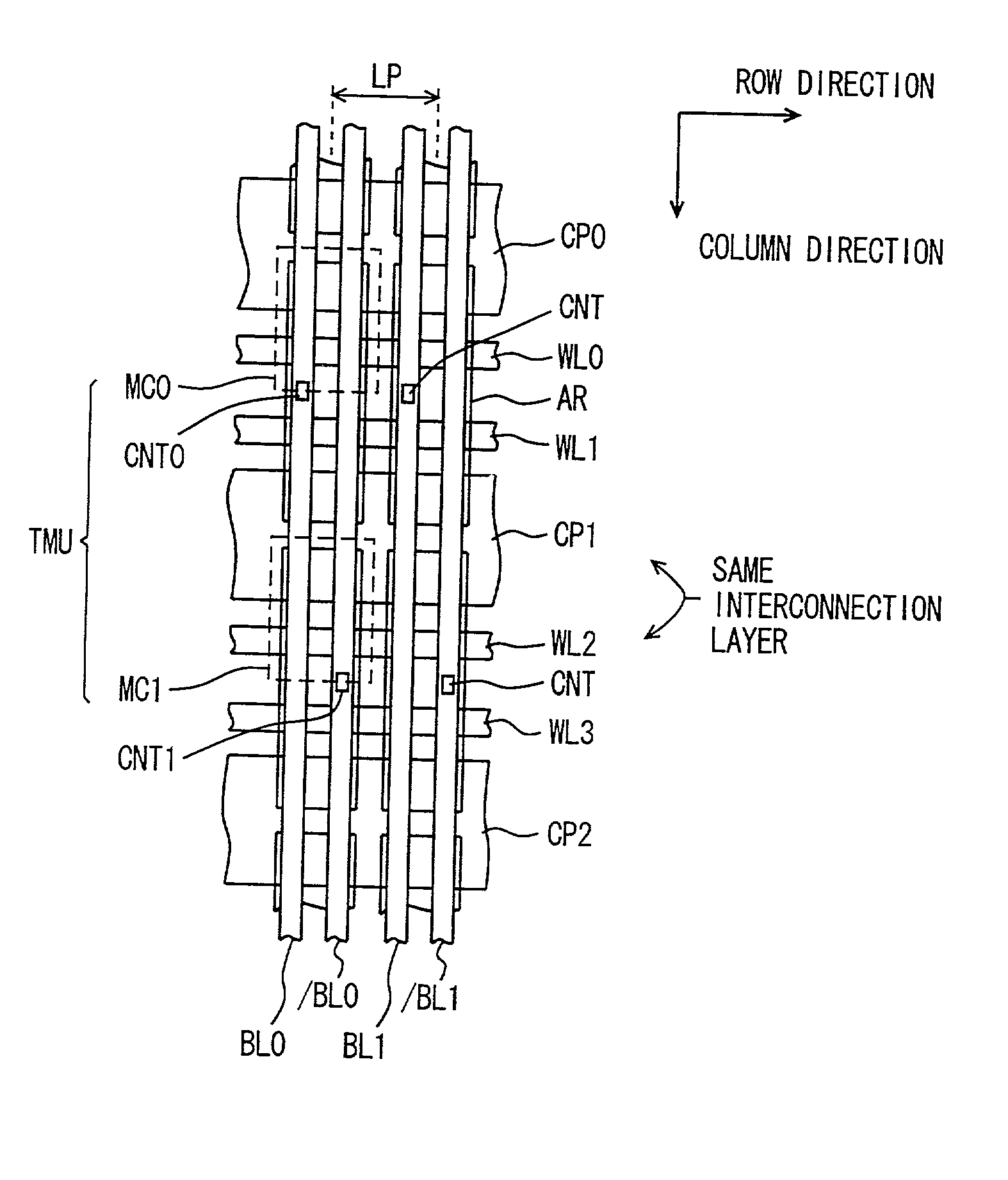
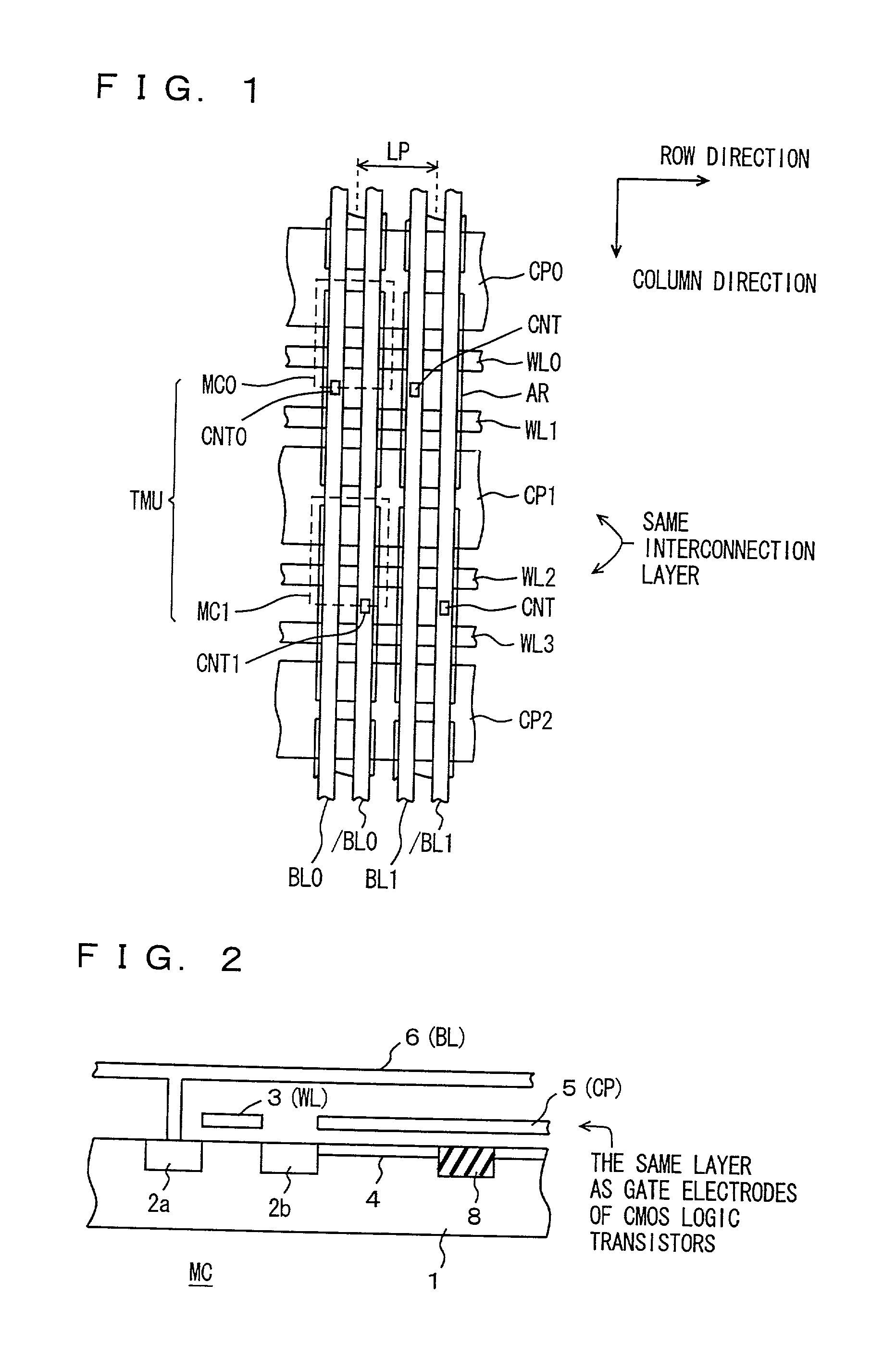
[0234] FIG. 24 is a diagram schematically showing a layout of a memory cell array according to a fourth embodiment of the present invention. In FIG. 24, active areas AR are arranged in alignment along the column direction. In each active area AR, 2-bit memory cells adjacent in the column direction are formed similarly to the third embodiment. Bit lines BL0 and / BL0 are arranged along the column direction in alignment with active areas AR. Therefore, one bit line is arranged at the pitch of the memory cells in the row direction. Thus, the pitch condition on the bit lines can be relaxed.

[0235] A memory cell MC0 is connected to a bit line BL0 through a contact CNT, and a memory cell MC2 is connected to a bit line / BL0 through a contact. When a word line WL1 is selected, data in memory cells MC0 and MC2 are read out onto bit lines BL0 and / BL0, respectively. Accordingly, in the case that data are stored in the twin cell mode, a twin cell unit is provided by mem...

fifth embodiment

[0242] [Fifth Embodiment]

[0243] FIG. 27 is a diagram schematically showing a layout of an array section of a semiconductor memory device according to a fifth embodiment of the present invention. In FIG. 27, active areas AR are arranged extending continuously in the column direction. With two bit lines provided for each of these active areas AR, the bit lines are arranged extending in the column direction in alignment with active areas AR.

[0244] Similarly to the above-mentioned embodiments, cell plate electrode lines CP0-CP2 and word lines WL are formed in the same interconnection layer in the row direction.

[0245] In the layout illustrated in FIG. 27, active areas AR are continuously extends in the column direction, and DRAM cells sharing a cell plate electrode line share a capacitor. Thus, each of unit memory cells MC4 and MC5 is formed in an area surrounded by contacts at both sides of cell plate electrode CP1. At both sides of each of the contacts, word lines WL0b and WL1a, or wor...


PUM


Abstract

Conductive lines constituting word lines of memory cells and conductive lines constituting memory cell plate electrodes are formed in the same interconnecting layer in a memory device including a plurality of memory cells each including a capacitor for storing data in an electrical charge form. By forming the capacitors of the memory cells into a planar capacitor configuration, a step due to the capacitors is removed. Thus. a dynamic semiconductor memory device can be formed through CMOS process, and a dynamic semiconductor memory device suitable for merging with logic is achieved. Data of 1 bit is stored by two memory cells, and data can be reliably stored even if the capacitance value of the memory cell is reduced due to the planar type capacitor.

Description

[0001] 1. Field of the Invention[0002] The present invention relates to a semiconductor memory device, and particularly to a semiconductor memory device having memory cells storing data in capacitors.[0003] 2. Description of the Background Art[0004] In a data processing field and the like, a circuit device called a system LSI large-scale integrated circuit), wherein a memory device and a logic such as a processor are integrated in the same semiconductor chip, has been widely used in order to process data at a high speed with low power consumption. In the system LSI, the logic and the memory device are interconnected through on-chip interconnect lines. Therefore, the system LSI has the following advantages: (1) since the load of the signal interconnection lines is smaller than that of on-board interconnection lines, data / signals can be transmitted at a high speed; (2) since the number of pin terminals is not limited, the number of data bits can be made large so that the band width in...

Claims


Application Information

Patent Timeline
IPC IPC(8): G11C11/404G11C11/401G11C11/405G11C11/407G11C11/409G11C11/4097H01L21/8242H01L27/10H01L27/108
CPCG11C7/18G11C8/14G11C11/4085G11C11/4087G11C11/4097G11C2211/4013H01L27/108H01L27/1085H01L27/10873H01L27/10882H01L27/0207H10B12/00H10B12/03H10B12/05H10B12/48
Inventor ARIMOTO, KAZUTAMISHIMANO, HIROKI
Owner RENESAS ELECTRONICS CORP
Why Eureka
Try Eureka