Nitride semiconductor light-emitting device and opticfal device and light-emitting apparatus with the nitride semiconductor light-emitting device

Inactive Publication Date: 2003-01-02
SHARP FUKUYAMA LASER CO LTD
View PDF2 Cites 36 Cited by
  • Summary
  • Abstract
  • Description
  • Claims
  • Application Information

AI Technical Summary

Problems solved by technology

Such a separation into different crystal systems causes decrease in the emission efficiency due to the deteriorated crystallinity.
A thickness of the well layer that is smaller than 0.4 nm increases, to an excessive degree, the carrier confinement level accomplished by the quantum well effect, resulting in decrease in the emission efficiency, and thus such a thickness is not preferable.
One possible reason, however, is that, concentration separation of element X could occur in the well layer even if the atomic percent of element X in the well layer is 30% or lower, the region where the concentration separation occurs gradually expands as the thickness of the well layer increases and, finally, the different concentrations of element X in the same well layer increases to such a degree that the characteristics of the light-emitting device are adversely affected.
Another possible reason is that, a very small region where crystal system separation occurs is generated in the well layer, the region of crystal system separation expands as the thickness of the well layer increases and, finally the crystal system separation advances to such a degree that the characteristics of the light-emitting device are adversely affected.
However, the concentration separation and crystal system separation to an excessive degree could deteriorate the characteristics of the light-emitting device.
Although it is uncertain why the thickness of the well layer has a significant influence on this structure of the light-emitting layer, one possible reason is that, when the GaN barrier layer is used, the steepness of the interface between the well layer and the GaN barrier layer is likely to be imp

Method used


Image

  • Nitride semiconductor light-emitting device and opticfal device and light-emitting apparatus with the nitride semiconductor light-emitting device
  • Nitride semiconductor light-emitting device and opticfal device and light-emitting apparatus with the nitride semiconductor light-emitting device
  • Nitride semiconductor light-emitting device and opticfal device and light-emitting apparatus with the nitride semiconductor light-emitting device

Examples


embodiment 2

[0071] In the device shown in FIG. 1, GaN substrate 100 is replaced with a pseudo GaN substrate 200 shown in FIG. 2 or a pseudo GaN substrate 200a shown in FIG. 3B, and an n-type electrode is formed on one side of the device as shown in FIG. 4. A nitride semiconductor laser device is accordingly fabricated similarly to Embodiment 1 except for above details.

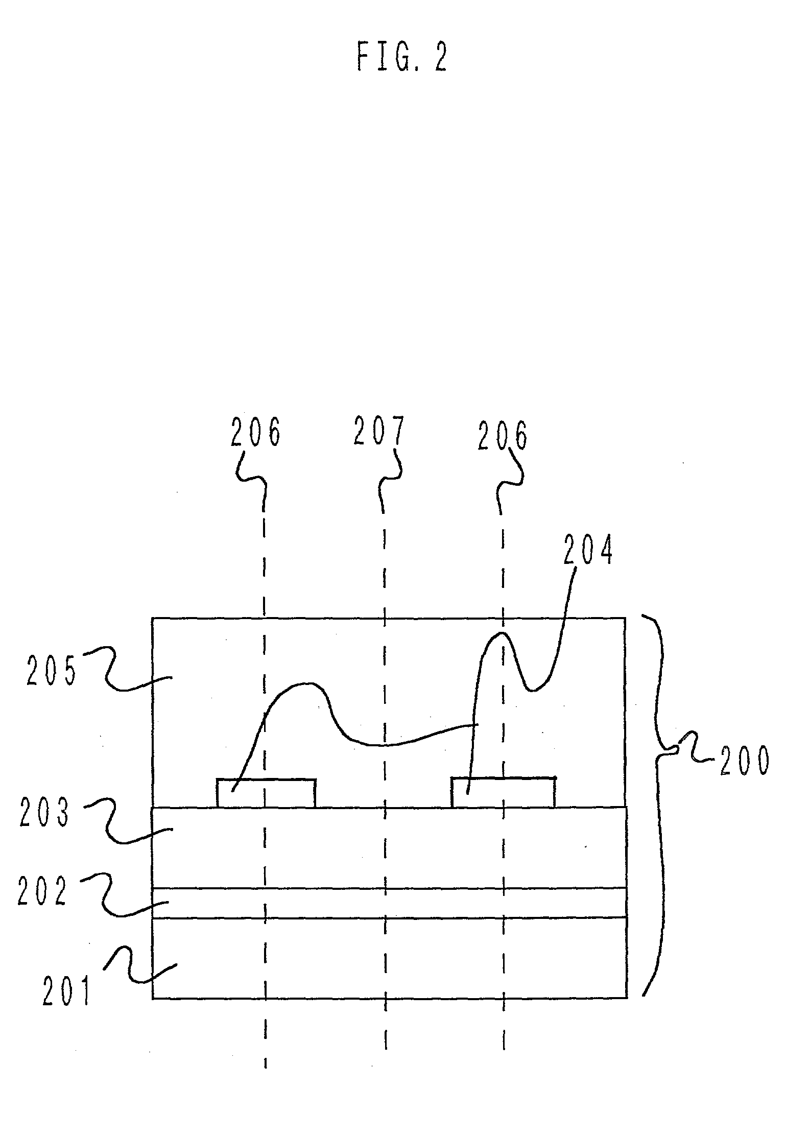
[0072] Pseudo GaN substrate 200 shown in FIG. 2 is constituted of a seed substrate 201, and a low temperature buffer layer 202, an n-type GaN layer 203, an anti-growth layer 204 and an n-type GaN thick layer 205 that are formed on seed substrate 201. Seed substrate 201 is used as a parent material on which n-type GaN thick layer 205 is grown. Anti-growth layer 204 is used for preventing the nitride semiconductor crystal layer from growing directly on the underlayer. Crystal growth through anti-growth layer 204 allows the growth to selectively be done in a specific crystal orientation. Any pseudo GaN substrate except for the one sh...

embodiment 3

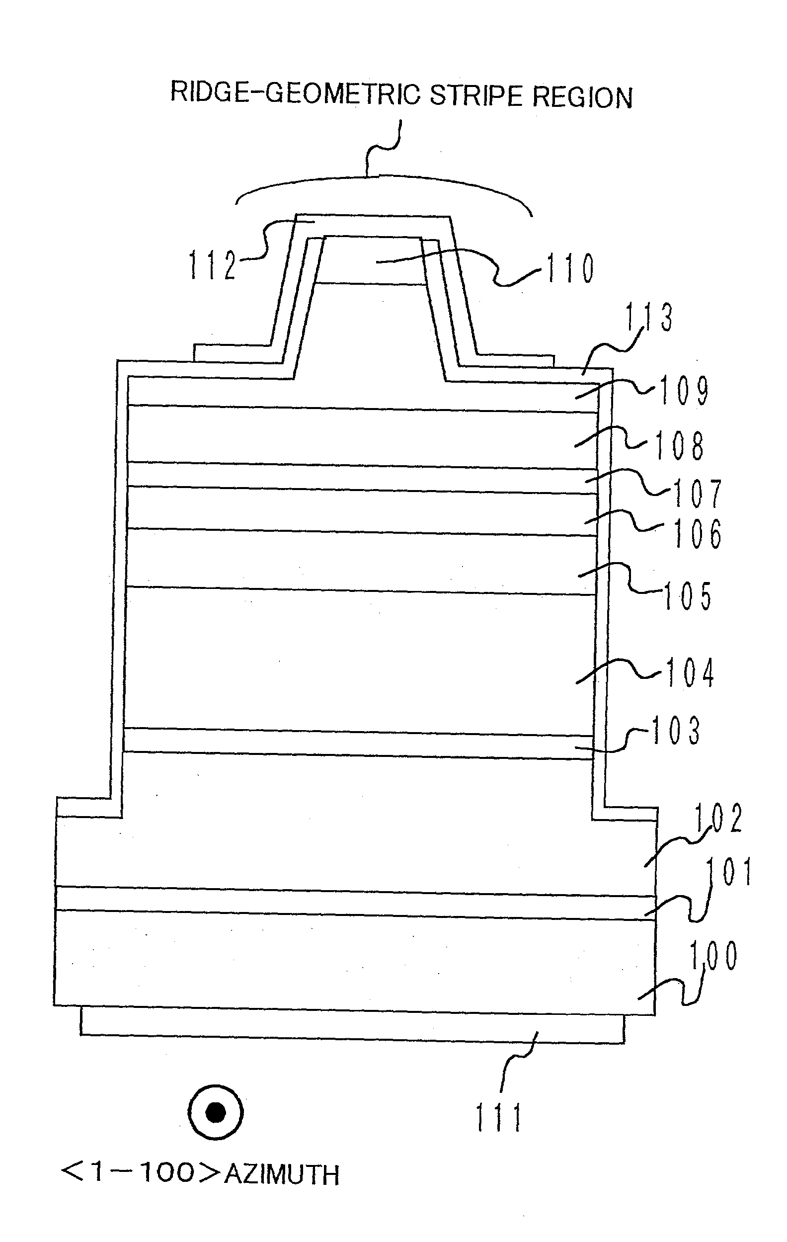
[0082] According to this embodiment, a nitride semiconductor laser device is produced in a similar manner to that of Embodiment 1 except that the nitride semiconductor laser device is formed on a hetero-substrate with a nitride semiconductor buffer layer therebetween and that an n-type electrode is formed on one side as shown in FIG. 4. The nitride semiconductor laser device thus produced has the structure as shown in FIG. 4 and includes a substrate 300, a low temperature GaN buffer layer 101 (thickness 25 nm), and n-type GaN layer 102, an n-type In.sub.0.07Ga.sub.0.93N anti-crack layer 103, an n-type Al.sub.0.1Ga.sub.0.9N cladding layer 104, an n-type GaN optical guide layer 105, a light-emitting layer 106, a p-type Al.sub.0.2Ga.sub.0.8N carrier blocking layer 107, a p-type GaN optical guide layer 108, a p-type Al.sub.0.1Ga.sub.0.9N cladding layer 109, a p-type GaN contact layer 110, an n-type electrode 111, a p-type electrode 112, and an SiO.sub.2 dielectric layer 113. Here, subst...

embodiment 4

[0085] A nitride light-emitting diode device is provided according to this embodiment. The light-emitting diode device shown in FIG. 5 includes an n-type GaN substrate 600 having C-plane (0001), a low temperature GaN buffer layer 601 (thickness 100 nm), an n-type GaN layer 602 (thickness 3 .mu.m, Si impurity concentration 1.times.10.sup.18 / cm.sup.3), a light-emitting layer 603 (5 cycles of GaN.sub.0.97As.sub.0.03 well layer (thickness 3.1 nm) / GaN barrier layer (thickness 6 nm)), a p-type Al.sub.0.1Ga.sub.0.9N carrier blocking layer 604 (thickness 20 nm, Mg impurity concentration 6.times.10.sup.19 / cm.sup.3), a p-type GaN contact layer 605 (thickness 0.1 .mu.m, Mg impurity concentration 1.times.10.sup.20 / cm.sup.3), a light-transmissive electrode 606, a p-type electrode 607, and an n-type electrode 608.

[0086] According to this embodiment, n-type electrode 608 is formed on the rear side of n-type GaN substrate 600 in the order of Hf / Al. Instead of this material for the n-type electrode,...


PUM


Abstract

A light-emitting device has a light-emitting layer of nitride semiconductor containing As, P or Sb and accordingly its emission efficiency or emission intensity is enhanced. The light-emitting device includes a substrate, and further includes n-type and p-type nitride semiconductor layers and a light-emitting layer between the n-type and p-type semiconductor layers that are formed on the substrate. Light-emitting layer includes one or a plurality of well layers formed of nitride semiconductor containing N and element X (element X is As, P or Sb). The nitride semiconductor of the well layer has at most 30% in atomic percent represented by expression {NX/(NN+NX)}x100 where NX represents the number of atoms of element X and NN represents the number of atoms of N. The thickness of the well layer ranges from 0.4 nm to 4.8 nm.

Description

[0001] 1. Field of the Invention[0002] The present invention relates to a nitride semiconductor light-emitting device as well as an optical device and a light-emitting apparatus that use the nitride semiconductor light-emitting device. In particular, the present invention relates to a nitride semiconductor light-emitting device having a high emission efficiency and to an optical device and a light-emitting apparatus with that nitride semiconductor light-emitting device.[0003] 2. Description of the Background Art[0004] Group V element such as As, P or Sb is added to gallium nitride-based compound semiconductor. Then, a resultant mixed crystal exhibits a great change in the bandgap with respect to a small change in the lattice constant. In consideration of this phenomenon, the amount of As, P or Sb to be added to the gallium nitride-based compound semiconductor, which constitutes a light-emitting layer, can be varied to change the emission wavelength. For example, Japanese Patent Layi...

Claims


Application Information

Patent Timeline
IPC IPC(8): H01L33/06H01L33/32H01S5/323H01S5/343
CPCH01L33/06H01L33/32
Inventor TSUDA, YUHZOHITO, SHIGETOSHI
Owner SHARP FUKUYAMA LASER CO LTD
Why Eureka
Try Eureka