
Photoelectric device

Inactive Publication Date: 2003-01-09
NIPPON SHEET GLASS CO LTD
View PDF0 Cites 21 Cited by
  • Summary
  • Abstract
  • Description
  • Claims
  • Application Information

AI Technical Summary

Benefits of technology

[0008] Therefore, with the foregoing in mind, it is an object of the present invention to provide a photoelectric conversion device that includes a photoelectric conversion layer having high photoelectric conversion efficiency even in a relatively long wavelength region, i.e., a photoelectric conversion layer having a relatively small band gap, and that is provided with a structure capable of improving the photoelectric conversion efficiency of the photoelectric conversion layer. In particular, it is an object of the present invention to provide a photoelectric conversion device that improves the photoelectric conversion efficiency of a crystalline silicon based thin film photoelectric conversion unit without relying only on the light trapping effect obtained by a transparent conductive film.

Problems solved by technology

However, when the film thickness is increased simply to increase optical absorption, the manufacturing cost becomes higher.
However, a conventional photoelectric conversion device is not always provided with a structure suitable for the characteristics of its photoelectric conversion layer.
However, this may degrade the quality of a crystalline silicon based thin film to be formed on the transparent conductive film.
Even if the crystalline silicon based thin film is formed via other thin films, as in the tandem structure, the surface unevenness with a large degree of slope causes degradation in the crystallinity of the crystalline silicon.
Even when using a photoelectric conversion layer that renders the photoelectric conversion efficiency in a relatively long wavelength region important, the conventional photoelectric conversion unit does not always adjust properly the characteristics of other members and thin films to be used with the photoelectric conversion layer, particularly their transmittance and contributions to the light trapping effect in that wavelength region.

Method used


Image

  • Photoelectric device
  • Photoelectric device
  • Photoelectric device

Examples


Embodiment Construction

[0061] Hereinafter, the present invention will be described more specifically by way of example, but is not limited thereto.

[0062] Manufacture of Glass Sheet with Transparent Conductive Film

[0063] Sample 1

[0064] In a production line for float glass, a tin oxide film (SnO.sub.2 film), a silicon oxide film (SiO.sub.2 film), and a fluorine-containing tin oxide film (SnO.sub.2:F film) were formed in this order on a glass ribbon using a plurality of coaters arranged in a float bath. The glass ribbon is formed to have a thickness of 4 mm and the total amount of iron oxide of 0.01 wt % in terms of Fe.sub.2O.sub.3.

[0065] Specifically, the glass ribbon had a temperature of about 650.degree. C. immediately before reaching a coater located at the furthest upstream position, and a mixed gas of dimethyltin dichloride (vapor), oxygen and nitrogen was supplied from the coater, so that a SnO.sub.2 film having a thickness of 25 nm was formed on the glass ribbon. Then, a mixed gas of monosilane, ethy...


PUM

PropertyMeasurementUnit
Fractionaaaaaaaaaa
Transparencyaaaaaaaaaa
Nanoscale particle sizeaaaaaaaaaa

Abstract

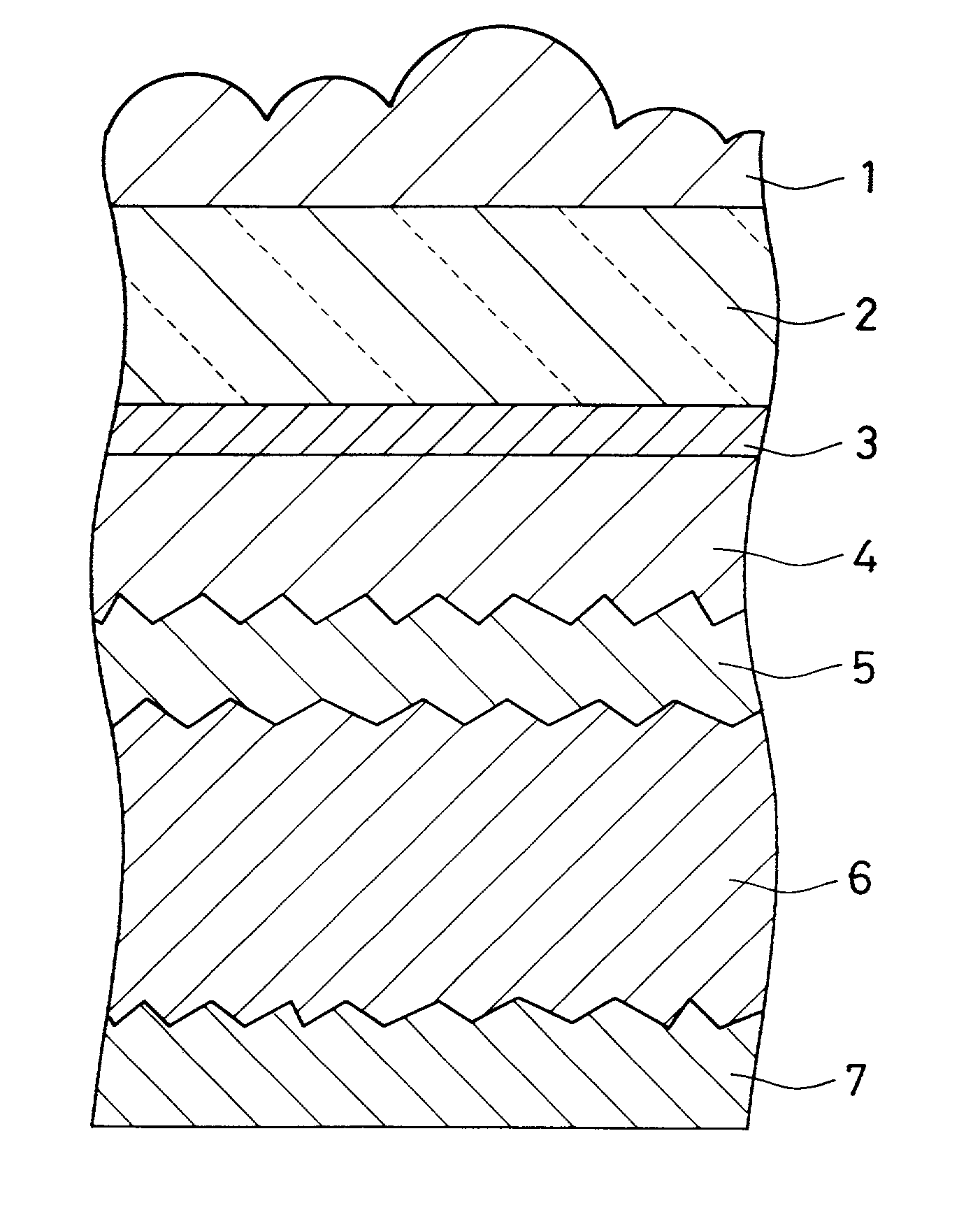
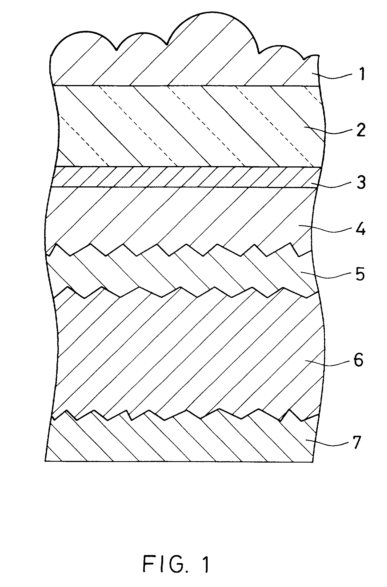
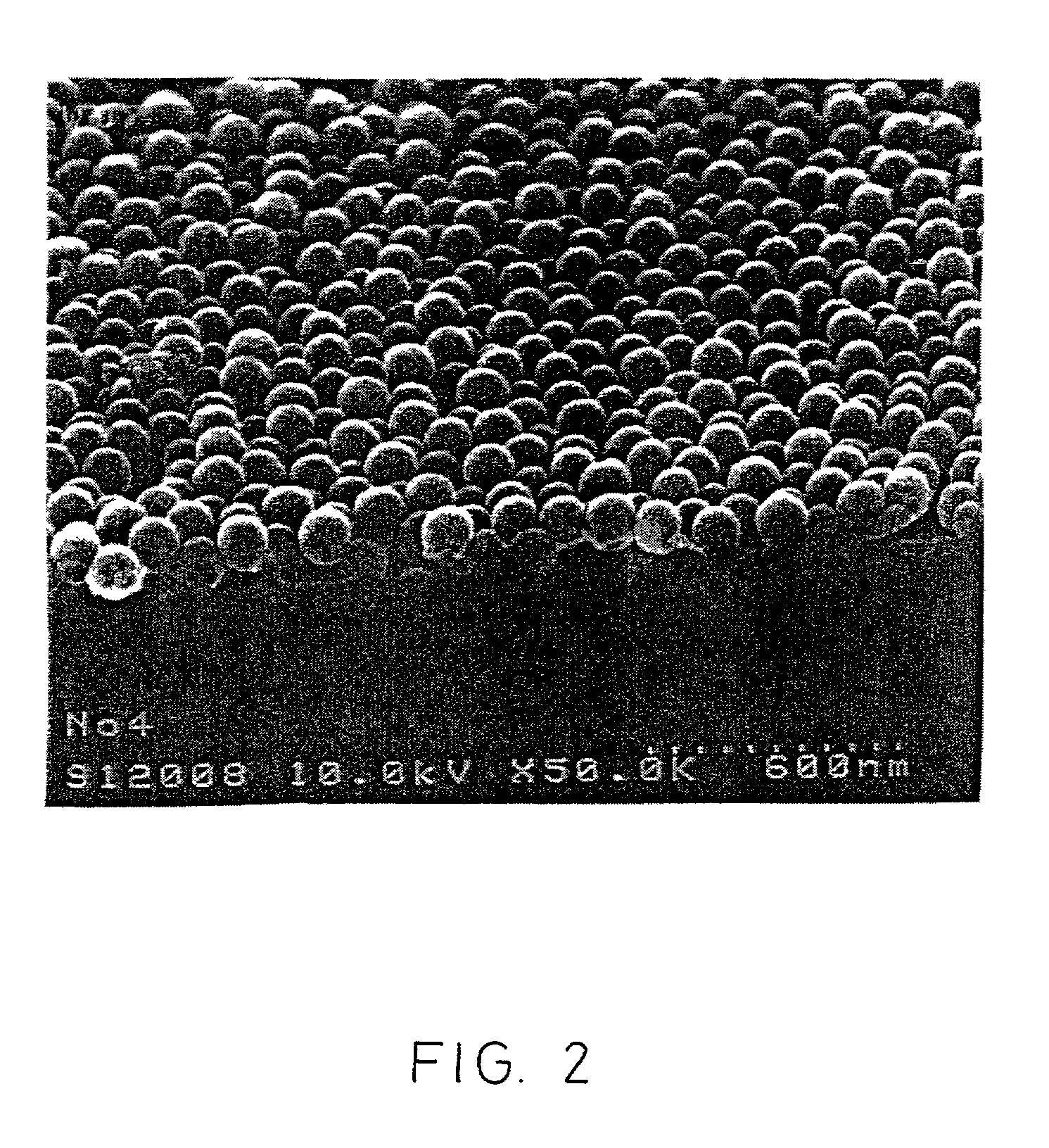
The present invention provides a photoelectric conversion device that improves photoelectric conversion efficiency with the interaction between a transparent substrate with a transparent conductive film, an antireflection film, and a photoelectric conversion unit. The antireflection film contains fine particles having an average particle diameter of 0.01 to 1.0 mum and has an uneven surface derived from the fine particles. The glass sheet with a transparent conductive film has a light transmittance of 75% or more in the wavelength region of 800 nm to 900 nm. The photoelectric conversion unit includes at least a photoelectric conversion unit including a photoelectric conversion layer having a band gap of 1.85 eV or less.

Description

[0001] The present invention relates to a photoelectric conversion device. More specifically, the present invention relates to a photoelectric conversion device including a photoelectric conversion layer of semiconductor material that has a relatively small band gap and photosensitivity even in a longer wavelength region.[0002] In a thin film-type photoelectric conversion device that uses a glass sheet as a substrate, a transparent conductive film, acting as a transparent electrode, is formed on the glass sheet, and a thin film photoelectric conversion unit including a photoelectric conversion layer is formed on the transparent conductive film. A tin oxide film often is employed as the transparent conductive film. The unevenness generated on the surface of the transparent conductive film with the growth of crystal grains has the effect of improving photoelectric conversion efficiency by trapping incident light in the photoelectric conversion layer or in the vicinity of the layer (i....

Claims


Application Information

Patent Timeline
IPC IPC(8): G02B1/11H01L31/0216
CPCG02B1/116H01L31/02161G02B1/111G02B1/02
Inventor HIRATA, MASAHIROOTANI, TSUYOSHITAWADA, YUKO
Owner NIPPON SHEET GLASS CO LTD
Learn More