
Semiconductor wafer plating cathode assembly

Inactive Publication Date: 2003-05-08
TELEDYNE SCI & IMAGING
View PDF0 Cites 43 Cited by
  • Summary
  • Abstract
  • Description
  • Claims
  • Application Information

AI Technical Summary

Benefits of technology

[0013] In a preferred embodiment, the seal to the wafer surface is provided by a polymer-coated metal ring having a sawtooth cross section so that force applied to compress the seal is concentrated along concentric circular ridges so as to provide maximum resistance to solution leakage past the seal. Use of multiple ridges provides redundancy, improving the seal effectiveness. For some applications, a single ridge or a flat seal may provide satisfactory results. Stainless steel is a preferred metal for fabricating the cathode assembly since it has the high strength needed for fabrication of stiff structures of minimum cross section. It also resists corrosion that could result from plating bath or rinse water contact, either directly or via pores in the polymer coating.
[0014] A preferred polymer coating material is polytetrafluoroethylene (PTFE), which is relatively soft and highly hydrophobic so that it tends to flatten in contact with the wafer surface and repel plating solution to form a very effective seal. It also provides outstanding protection and insulation to the metal since it is chemically inert and repels solution from pores in the coating due to its hydrophobicity. Very thin PTFE coatings applied by thermal spraying are highly adherent to stainless steel (and other metals). For improved seal performance and to suppress electroplating through pinholes, the PTFE coating can be thickened by multiple applications.

Problems solved by technology

A major problem with current wafer plating systems is that the gasket or o-ring used to form a seal to the wafer requires a reasonably thick mechanical support structure which protrudes past the wafer plated surface, impeding solution flow and causing nonuniform copper deposition.
Complicated baffles and shields are used in conjunction with cathode rotation to improve copper plating uniformity but these increase the complexity and expense of automation and do not provide optimum plating results.
In addition, the requirement of cathode rotation is more easily fulfilled by exposing the wafer to the solution in the plated-side-down configuration for which trapping of bubbles within fine trenches and vias is a problem.
Even if the coplanarity requirement within individual chips is met, too much solder in the balls can cause bridging that shorts the device.
On the other hand, too little solder can result in structurally unsound solder joints because of inadequate underfill in the narrow space available, diminished distance over which stresses caused by thermal expansion mismatches can be relieved, and / or solder joint embrittlement induced by excessive volume fraction of gold contamination from seed or barrier layers.

Method used


Image

  • Semiconductor wafer plating cathode assembly
  • Semiconductor wafer plating cathode assembly
  • Semiconductor wafer plating cathode assembly

Examples


Embodiment Construction

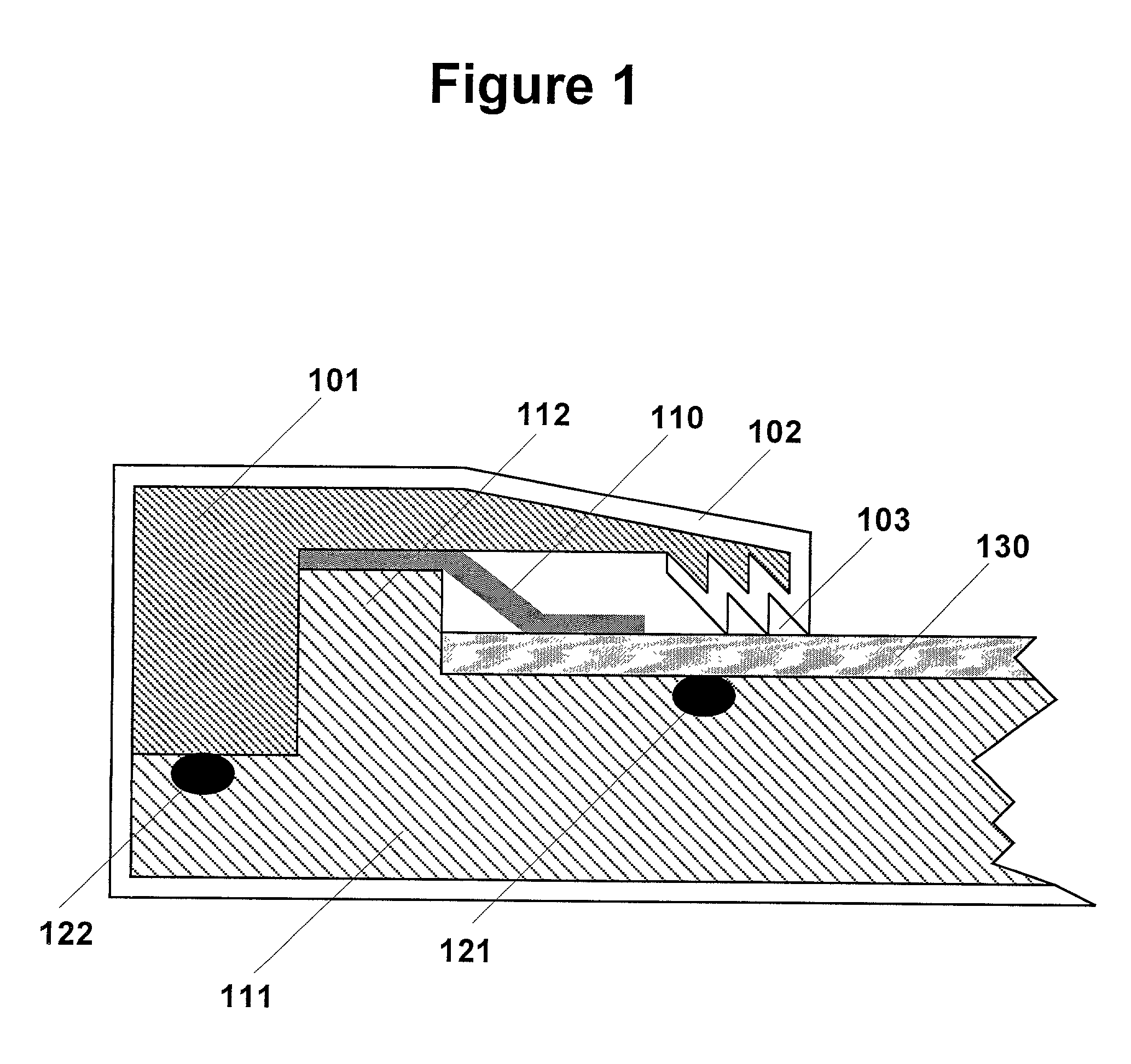
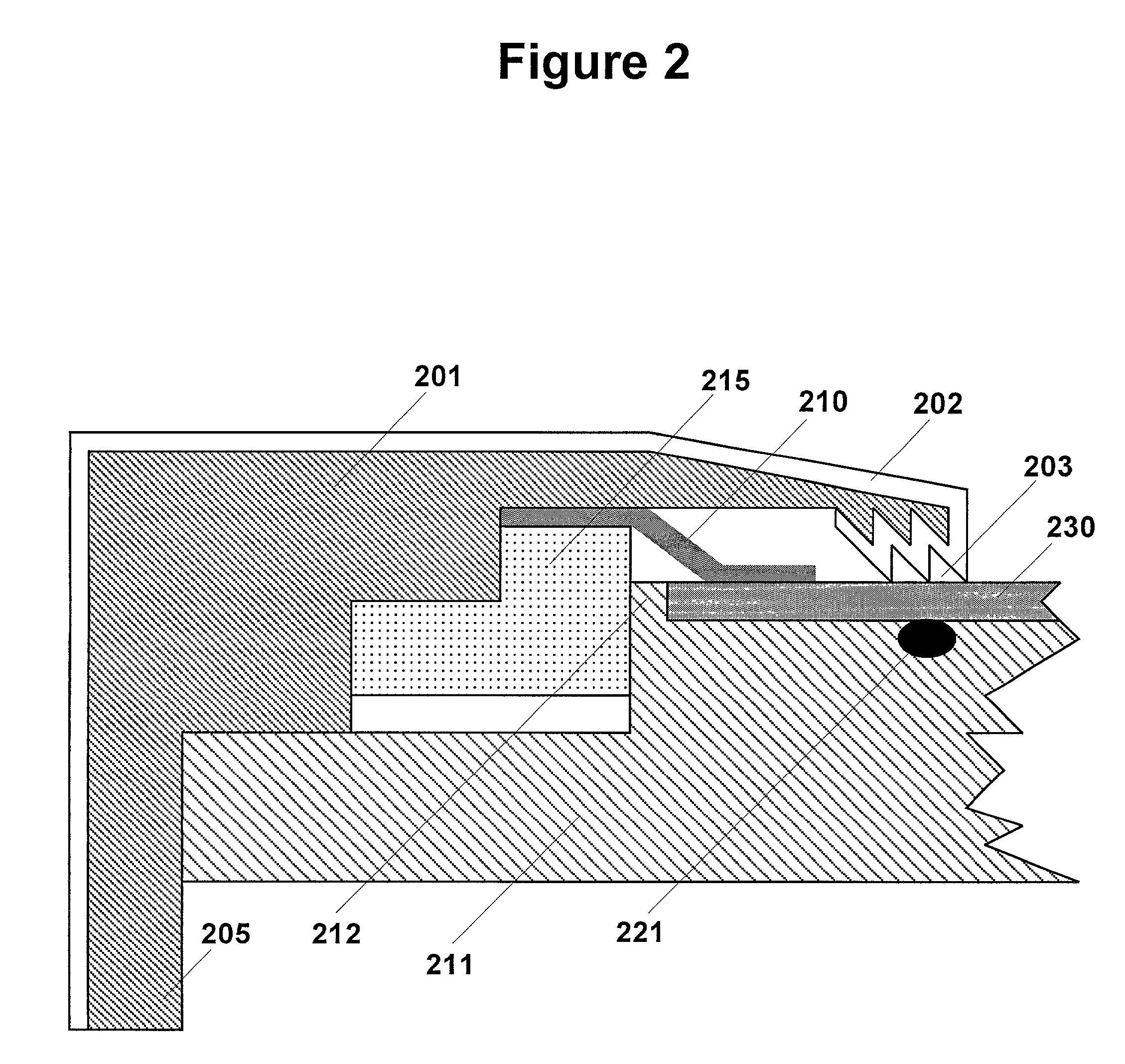
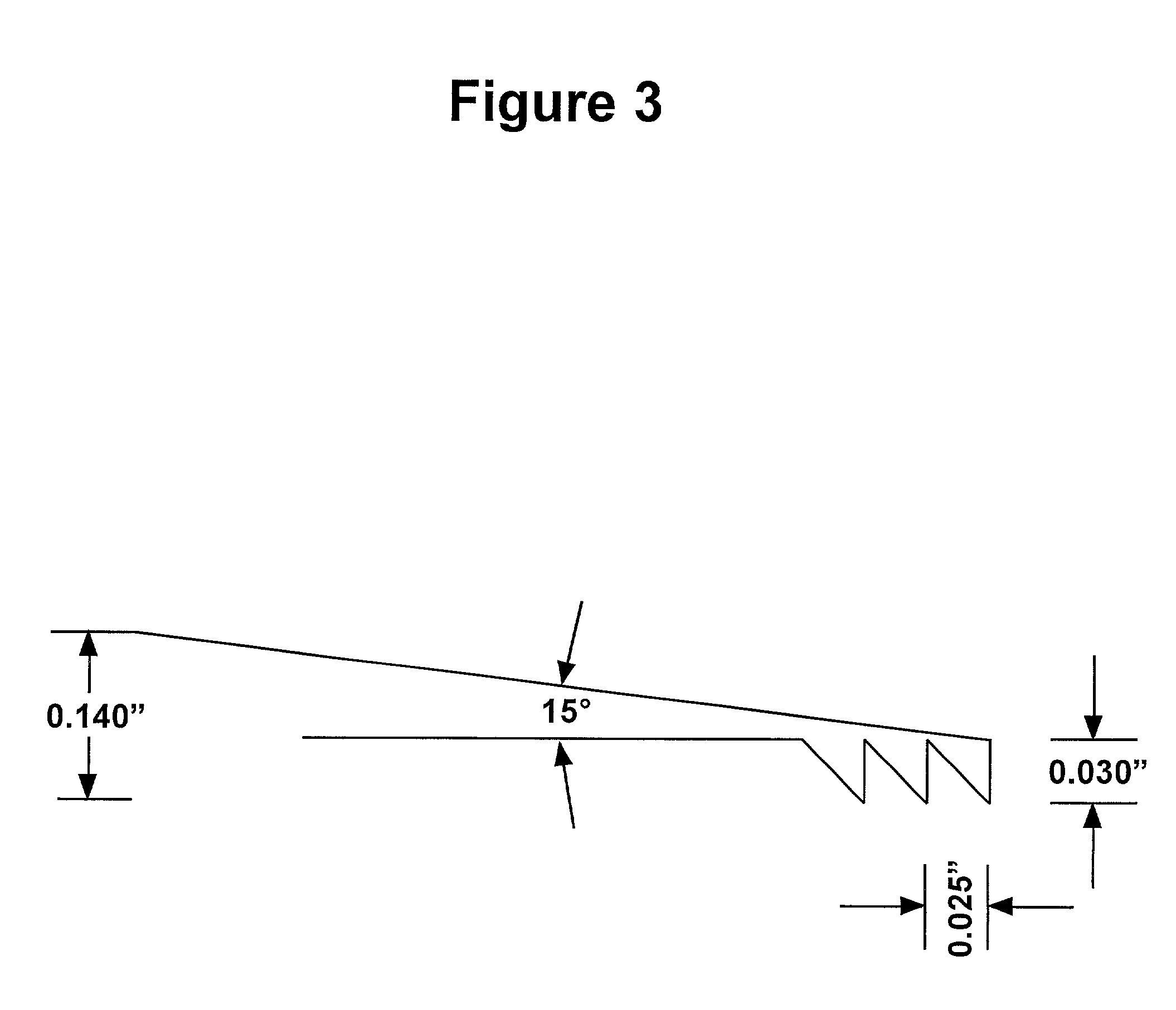
[0019] This invention is a cathode assembly for semiconductor wafer plating that employs an electrically-insulating coating on a ring-shaped electrically-conductive support structure to provide an improved seal to the perimeter area of the plated side of the wafer. The insulating coating performs the dual function of forming the wafer seal and electrically insulating the conductive support structure so that it can be used in contact with the plating solution and still be part of the electrical contact system. Since the coating used to form the seal can be very thin and can be supported by a relatively strong metal structure, the extent of protrusion of the cathode assembly above the wafer plated-side surface can be minimized. Likewise, such a polymer coated metal structure replaces both the plastic support and protective housing used in the prior art so that the overall dimensions of the assembly can be significantly reduced. Such a compact cathode assembly with minimum protrusion a...


PUM

PropertyMeasurementUnit
Thicknessaaaaaaaaaa
Flow rateaaaaaaaaaa
Diameteraaaaaaaaaa

Abstract

A cathode assembly for semiconductor wafer plating employs a polymer coating on a metal structural ring to provide a low-profile seal to the perimeter of the wafer surface to be plated. The polymer coating also electrically insulates the metal so that it can be used in contact with the plating solution and still be part of the electrical contact system, eliminating the need for a protective plastic housing. This invention permits the dimensions of the cathode assembly to be minimized. A compact cathode assembly with minimum protrusion above the wafer plated surface enables modifications to the plating cell and agitation system providing more uniform copper deposits across the wafer surface and facilitating automation of the wafer plating process.

Description

[0001] This application is related to an application of D. Morgan Tench and John T. White entitled "Improved Semiconductor Wafer Plating Cell Assembly", which is being filed on the same date as this application.[0002] 1. Field of the Invention[0003] This invention is concerned with electroplating of semiconductor wafers, and in particular with the formation of copper integrated circuits (IC's) on semiconductor chips.[0004] 2. Related Prior Art[0005] The electronics industry is in the process of transitioning from aluminum to copper as the basic metallization for semiconductor IC's. The higher electrical conductivity of copper reduces resistive losses and enables the faster switching needed for future generations of advanced devices. Copper also has a higher resistance to electromigration than aluminum.[0006] The leading technology for fabricating copper circuitry on semiconductor chips is the "Damascene" process (see, e.g., P. C. Andricacos, Electrochem. Soc. Interface, Spring 1999,...

Claims


Application Information

Patent Timeline
IPC IPC(8): C25D7/12C25D17/06H01L21/288
CPCH01L21/2885C25D17/06
Inventor DAVIS, GREGMOFFATT, ALEXTENCH, D. MORGANWHITE, JOHN T.
Owner TELEDYNE SCI & IMAGING
Features
  • Generate Ideas
  • Intellectual Property
  • Life Sciences
  • Materials
  • Tech Scout
  • Unparalleled Data Quality
  • Higher Quality Content
  • 60% Fewer Hallucinations
Learn More