Semiconductor module substrate sheet, semiconductor module substrate sheet fabricating method and semiconductor module

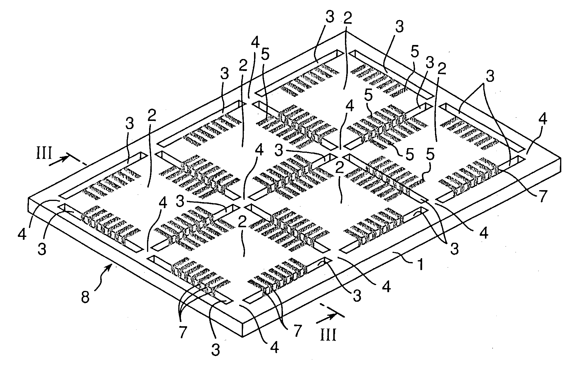
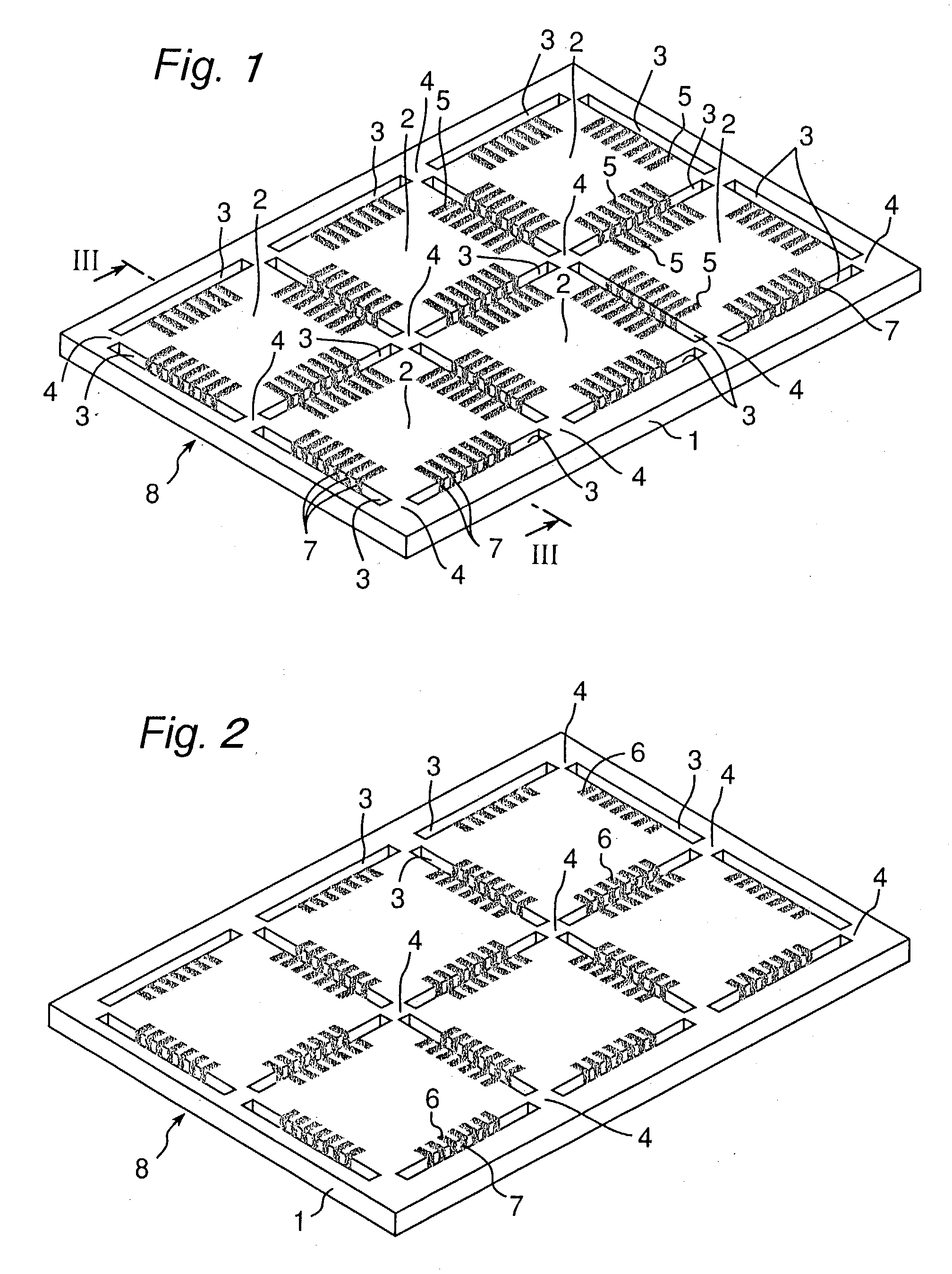
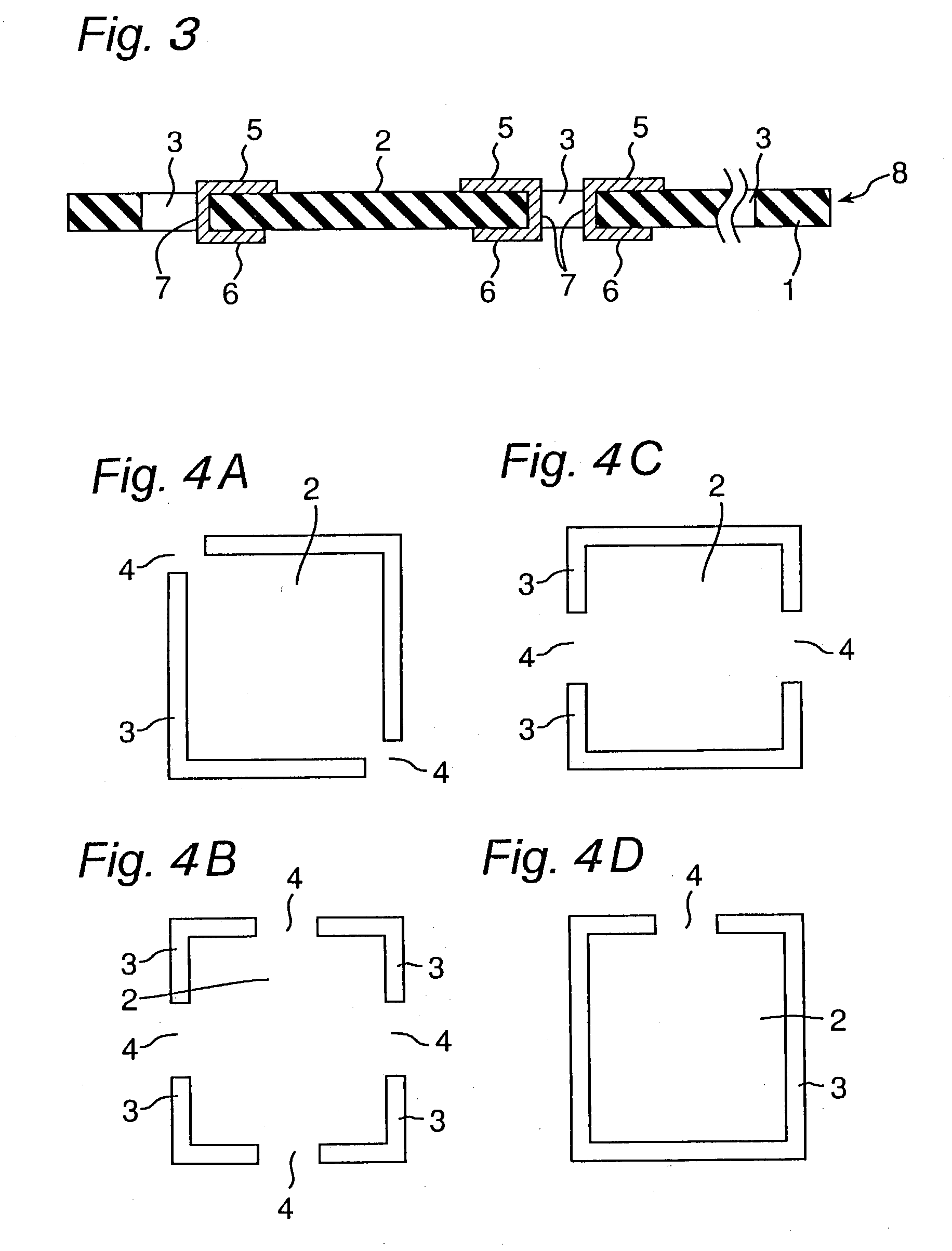
a technology of semiconductor modules and substrate sheets, applied in the direction of instruments, circuit masks, photo-taking processes, etc., can solve the problems of bending and bonding of films, frame thickness has not been reduced, and pure copper, which has good electrical conductivity, etc., to reduce processing efforts, reduce the number of through holes 3k, and reduce the cost

Inactive Publication Date: 2003-08-21
NISSHA PRINTING COMPANY
View PDF3 Cites 18 Cited by
  • Summary
  • Abstract
  • Description
  • Claims
  • Application Information

AI Technical Summary

Benefits of technology

[0154] As a semiconductor module substrate sheet 8a according to a modified example of the first embodiment of the present invention, as shown in FIG. 5, a recess 9 of a size capable of receiving a semiconductor chip 10 may be provided at the center of each semiconductor chip placement region 2 on a surface thereof where the inner lead sections 5 are formed, so that the semiconductor chip 10 is received and held in the recess 9, allowing the semiconductor chip 10 to be more stably supported on the substrate sheet 8a.
[0275] Likewise, the lead pattern shielding-sections 33f are formed by patterning in correspondence with the inner lead sections 5, while the connection pattern shielding-sections 33g are formed by patterning in correspondence with the connecting sections 7 to be connected to the inner lead sections 5 and connected to the lead pattern shielding-sections 33f. The lead pattern shielding-sections 33h are formed by patterning in correspondence with the outer lead sections 6. However, the present invention is not limited to this. That is, by reversing the positional relation of the two masks 33 with respect to the substrate 38, it is acceptable to form by patterning the lead pattern shielding-sections 33f in correspondence with the outer lead sections 6, form by patterning the connection pattern shielding-sections 33g in correspondence with the connecting sections 7 to be connected to the outer lead sections 6 for connection of the connection pattern shielding-sections 33g to the lead pattern shielding-sections 33f, and form by patterning the lead pattern shielding-sections 33h in correspondence with the inner lead sections 5. Except for the case where the scrapping-off is performed physically means such as with a laser, these methods, through exposure to light can expose the inner lead sections, the connecting sections, and the outer lead sections through a continuous process or concurrently, allowing the inner lead sections, the connecting sections and the outer lead sections to be subjected to the formation of etching resist or plating resist through one development process. Therefore, the inner lead sections, the connecting sections, and the outer lead sections can be concurrently effectively formed at low cost by etching or plating.

Problems solved by technology

For the above reasons, the metallic lead frame has not been able to have a reduced thickness, and consequently, pure copper, which has good electrical conductivity, has been hard to use.
However, the above method, which requires many fabricating steps including the formation of the inner lead sections and the like on a film and then the bending and bonding of the film, has disadvantageously been troublesome.
In the case of the semiconductor package having an increased number of pins and narrower pitches as described above, even a slight error in positional alignment occurring in the film bending and bonding stages cannot be ignored, and this positional alignment error disadvantageously has caused difficulties in maintaining the dimensional accuracy.

Method used


Image

  • Semiconductor module substrate sheet, semiconductor module substrate sheet fabricating method and semiconductor module
  • Semiconductor module substrate sheet, semiconductor module substrate sheet fabricating method and semiconductor module
  • Semiconductor module substrate sheet, semiconductor module substrate sheet fabricating method and semiconductor module

Examples


working example 2

[0284] A BT resin double-sided substrate CCLHL-830 (having a thickness of 0.1 mm and a copper foil of 18 .mu.m on both sides) having a size of 340 mm.times.255 mm, produced by MITSUBISHI GAS CHEMICAL CO., INC. is prepared. An array in which eight semiconductor chip placement regions, each having a size of 2.4 mm long.times.3 mm wide, are arranged at a pitch of 3 mm in the lateral direction and 41 semiconductor chip placement regions are arranged at a pitch of 2.4 mm in the longitudinal direction is used as one set. Six sets in the lateral direction by 3 sets in the longitudinal direction of the semiconductor chip placement regions are arranged, and through holes of 0.9 mm wide.times.25 mm long are provided by punching on the sides in the lateral direction of the semiconductor chip placement region owned by each set (note that each through hole has a length 0.5 mm longer than that of the semiconductor chip placement region at both ends). In other words, through holes are provided on ...

working example 3

[0290] As a substrate material, a 0.1-mm thick plate made of glass cloth-incorporated BT (bismaleimide-triazine) resin produced by MITSUBISHI GAS CHEMICAL CO., INC. laminated with a 0.018-mm thick Cu foil on both surfaces thereof is used. As a metal layer, an 18-.mu.m thick Cu layer is formed by electroless plating and electroplating. As a resist, a positive type electrodeposition etching resist (photolysis type) produced by NIPPON PAINT CO., LTD is coated. The thickness is 0.007 mm to 0.008 mm. Exposure is performed at 600 mJ / cm.sup.2 with a high-pressure mercury lamp. Development is carried out at 32.degree. C. with 1% sodium metasilicate enneahydrate aqueous solution being sprayed. This is carried out for about 60 seconds. Etching is carried out at 50.degree. C. with 45-Baume ferric chloride aqueous solution being sprayed. This is carried out for about four minutes. Resist removal is carried out by immersion in a 3-5% caustic soda aqueous solution at normal temperature for about ...


PUM

PropertyMeasurementUnit
sizeaaaaaaaaaa
thicknessaaaaaaaaaa
sizeaaaaaaaaaa

Abstract

Through holes are formed at four peripheral edges of a plurality of semiconductor chip placement regions of an insulating substrate, except for coupling portions partially arranged thereat. A substrate sheet for semiconductor module is used in which connecting portions between inner lead portions and outer lead portions arranged on both surfaces of the substrate are formed in pattern on the side wall surface of the through hole. The semiconductor chip is mounted on each region, electrode terminals thereof and the inner lead portions are electrically connected to each other, the chip is sealed, and then the coupling portions are cut.

Description

[0001] This application is a divisional application of Ser. No. 09 / 601,766, filed Aug. 8, 2000 which is a national stage application of International Application Number PCT / JP99 / 00576 filed on Feb. 10, 1999.[0002] The present invention relates to a semiconductor module substrate sheet that constitutes a semiconductor module with one or a plurality of semiconductor chips of monolithic IC's, hybrid IC's, multi-tip IC's, diodes, transistors, thyristors, or the like mounted thereon, a method for fabricating the semiconductor module substrate sheet and a semiconductor module constructed of the substrate sheet mounted with semiconductor chips mounted thereon.[0003] Conventionally, a semiconductor package of a monolithic IC, a hybrid IC, a multi-tip IC, a diode, a transistor, a thyristor, or the like has been formed by punching by using a press, or by etching a metal conductor of a die pad and leads on which a semiconductor chip is mounted as represented by a lead frame, mounting the semic...

Claims


Application Information

Patent Timeline
Patent Type & Authority Applications(United States)
IPC IPC(8): H01L21/56H01L23/13H01L23/31H01L23/498H01L23/50H05K1/02H05K1/14H05K3/00H05K3/06H05K3/10H05K3/18H05K3/34H05K3/40
CPCH01L21/561H01L2924/1301H01L23/3121H01L23/49805H01L23/49838H01L23/50H01L24/97H01L2224/48091H01L2224/48227H01L2224/48465H01L2224/73265H01L2224/97H01L2924/01011H01L2924/01013H01L2924/01018H01L2924/01027H01L2924/01029H01L2924/01033H01L2924/01039H01L2924/01046H01L2924/01047H01L2924/01054H01L2924/01078H01L2924/01079H01L2924/01082H01L2924/15151H01L2924/3025H05K1/0206H05K1/141H05K3/0052H05K3/0082H05K3/064H05K3/108H05K3/184H05K3/3442H05K3/403H05K2201/049H05K2201/0959H05K2201/09645H05K2203/1407H01L2224/16225H01L2224/32225H01L24/48H01L2924/01005H01L2924/01006H01L2924/01019H01L2924/01023H01L2224/45144H01L2924/12041H01L2924/07811H01L23/13H01L2224/85H01L2924/00014H01L2224/81H01L2924/00H01L24/49H01L2224/49175H01L2924/12042H01L2924/181H01L2924/00012H01L2224/45099H01L2224/45015H01L2924/207
Inventor YAMAMOTO, KUNITOSHITSUJI, KOICHIRO
Owner NISSHA PRINTING COMPANY
Why Eureka
Try Eureka