
Attachment of surface mount devices to printed circuit boards using a thermoplastic adhesive

a technology of thermoplastic adhesive and printed circuit board, which is applied in the direction of dielectric characteristics, sustainable manufacturing/processing, and final product manufacturing, etc., can solve the problems of chip package/pcb solder joint failure, chip package/pcb solder joint adhesion becoming more problematic, and reducing the size of each solder ball and join

Inactive Publication Date: 2003-09-11
WESTLAKE EPOXY INC
View PDF13 Cites 56 Cited by
  • Summary
  • Abstract
  • Description
  • Claims
  • Application Information

AI Technical Summary

Benefits of technology

0024] c) heating the assembly under solder reflow conditions effective to provide an adhesive bond between the organic bottom surface of the electronic device and the printed circuit board and effective to provide a solder joint between the connecting substrate and the landing pads on the printed circuit board.
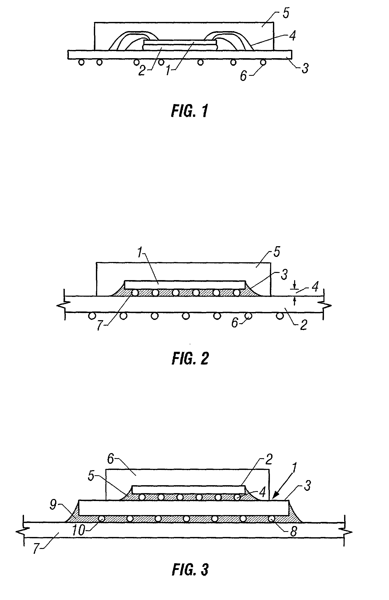
0025] In another process embodiment, there is provided a process for adhering a printed circuit board comprising landing pads to a surface mount electronic device comprising a connecting substrate having a bottom surface with leads, said process comprising adhering a thermoplastic adhesive onto a portion of said bottom surface, mounting the electronic device onto a printed circuit board to form an assembly in which the leads on said bottom surface are aligned with corresponding landing pads and the thermoplastic adhesive faces the printed circuit board forming a gap between the thermoplastic adhesive and the printed circuit board, followed by heating the assembly under solder reflow conditions effective to provide an adhesive joint between said bottom surface and the printed circuit board, wherein the thermoplastic adhesive comprises a functionalized polyolefin.
0026] There is also provided a process for adhering a printed circuit board comprising landing pads to a surface mount electronic device comprising a connecting substrate having a bottom surface with leads, said process comprising adhering a thermoplastic adhes...

Problems solved by technology

These hand held devices are subject to impact by drops or vibration, leading to the failure of the chip package / PCB solder joint.
Adhesion of the chip package to the PCB is becoming more problematic as the technology continues to miniaturize the chip packages, the interconnect density increases, the solder ball density decreases thereby reducing the size of each solder ball and joint, and the gap between the chip package and the PCB continues to decrease.
However, the vibration and drop resistance is not sufficient and the electrically connected solder joints fail.
The addition of metal grids and springs to act as shock absorbers has been proposed, but this mechanical solution requires additional space by increasing gap distance and chip size.
However, the use of underfills has not provided a complete and economical solution to joint failure in a market which demands ever increasing performance at lower costs.
In addition to the problem of adhesion in new surface mounted technologies, the use of underfills introduced a costly and complex manufacturing step due to the specific material design need to achieve performance demands and the manufacturing cycle time.
The underfill technology also requires dispensing the resin uniformly throughout both surfaces of the gap, and throughout the whole of the surfaces, thus requiring the use of large amounts of material in the process.
Moreover, once hardened, most thermosetting resin bonds are permanent, so rework or repair of faulty chips or solder joints becomes impractical.

Method used


Image

  • Attachment of surface mount devices to printed circuit boards using a thermoplastic adhesive
  • Attachment of surface mount devices to printed circuit boards using a thermoplastic adhesive
  • Attachment of surface mount devices to printed circuit boards using a thermoplastic adhesive

Examples


working examples

[0192] Films of test adhesives were prepared by placing about 1 gram of adhesive pellets on a TEFLON.TM. plate resting on top of an aluminum plate preheated in an oven to a temperature of about 200.degree. C. The pellets were allowed to heat for about 1 minute, after which a second TEFLON.TM. plate was laid on top of the molten pellets, followed by an aluminum plate weighted with a 5 lb copper bar. The assembly was allowed to heat for 10-15 minutes to about 200.degree. C., removed from the oven, clamped into a vise, and squeezed to form a 7 mil thick film. For thicker films in the range of 10-15 mils, 2 grams of the adhesive pellets were placed on the TEFLON.TM. plates in the oven, and the assembly was pressed with appropriately sized shims. From the cooled sheets, the adhesive strips or squares were cut to size.

[0193] FPE 1 is an acid functionalized polyethylene polymer functionalized with 10.5 wt % methacrylic acid having a melt index of 35.

[0194] FPE 2 is an acid functionalized p...

example 1

[0199] Thin strips measuring from 0.010" to 0.015" by 1 / 4" long were cut from the FPE 2 and the FPE 3 sheets. The FPE 2 strips were laid along the two parallel edges of a 1 / 4".times.1 / 4" glass slide 0.025" thick, and also along two parallel edges on a BGA. With the polyolefin side up, the polyolefins were bonded to the glass slides and the BGA by heating to the first stage of a Thermal Cycle. The Thermal Cycle apparatus used was a 1 / 4" TEFLON.TM. board mounted on a lift under a Dayton IR lamp equipped with 900 watt lamps. Using temperature probe thermal waxes, the distance to the heat lamp to achieve a temperature of 180.degree. C. was determined, and the time to reach 180.degree. C. was determined to be 255 seconds. Once the test sample was exposed to the heat lamp for 255 seconds, the test sample was heated in a second stage by elevating the lift to a distance from the lamp predetermined to reach 260.degree. C. within 45 seconds.

[0200] To bond the FPE 2 to the glass slide and the ...

example 2

[0204] FPE 2 adhesive was cut into 1 / 4" strips having a thickness of about 0.024", laid up along two parallel edges on a glass test slide measuring 1 / 4".times.1 / 4".times.0.040", and heat bonded to the slide by subjecting the slide, adhesive side up, to a first stage in a Thermal Cycle (ambient to 180.degree. C. over 255 seconds.). Once cooled, the glass slide was inverted, and mounted on top of a glass spacer sitting on the chip side of a printed circuit board wiped clean with acetone. The glass spacer was thick enough to provide a gap between the adhesive and the printed circuit board. The assembly was Thermally Cycled through both stages. Visual inspection revealed that the adhesive had sagged and flowed sufficiently to form a joint with the printed circuit board.

[0205] In the Mandrel bend test, the assembly passed through all deflections down to the 0.75" mandrel.


PUM

PropertyMeasurementUnit
Lengthaaaaaaaaaa
Fractionaaaaaaaaaa
Fractionaaaaaaaaaa

Abstract

An assembly having a surface mounted electronic device mounted onto a printed circuit board and a thermoplastic adhesive applied to the surface mounted electronic device facing the printed circuit board and providing for a gap between the thermoplastic adhesive and the printed circuit board. The assembly is heated at solder reflow temperatures to at least soften the thermoplastic adhesive sufficiently to flow across the gap and provide a thermoplastic adhesive joint between the surface mounted electronic device and the printed circuit board.

Description

1. FIELD OF THE INVENTION[0001] The invention relates to a process and material for adhering surface mounted electronic device to printed circuit boards, and more particularly to a process for adhering surface mounted electronic device to printed circuit board using a thermoplastic adhesive and thermoplastic adhesive compositions.2. BACKGROUND OF THE INVENTION[0002] In recent years, the demands for the miniaturization of electronic instruments, higher frequency processing speeds, weight savings, and reduction in manufacturing costs are driving down the solder bump density and requiring an increase on the number of solder bumps per package. The industry has progressed from the use of through hole pin technology in which the pin leads on the semiconductor package are physically inserted through corresponding holes in the printed circuit board (PCB), to surface mount technology (SMT) to improve both manufacturing costs and density.[0003] There exist numerous techniques for mounting sem...

Claims


Application Information

Patent Timeline
IPC IPC(8): H01L21/56H01L23/13H01L23/29H05K3/30
CPCH01L21/563H01L23/13H01L2924/10253H01L2924/01087H01L2924/01019H01L24/48H05K2201/10984H05K2201/10734H05K2201/0129H05K3/305H01L2924/19041H01L2924/15311H01L2924/01079H01L2924/01077H01L2924/01025H01L2924/0102H01L2924/01012H01L2224/73265H01L2224/73204H01L2224/73203H01L2224/48227H01L2224/48091H01L2224/32225H01L23/293H01L2224/16225H01L2924/00014H01L2924/00012H01L2924/00H01L2924/12042H01L24/73H01L2224/05599H01L2224/45099H01L2224/85399H01L2924/14H01L2924/181Y10T428/249985H01L2924/15153Y02P70/50H01L2224/45015H01L2924/207
Inventor STEWART, STEVEN L.ASH, CARLTON E.
Owner WESTLAKE EPOXY INC
Learn More