Photopic detector system and filter therefor
a detector system and detector technology, applied in the field of detector systems, can solve the problems of low transmission rate, inconvenient processing of glass in molding, cutting, polishing operations, etc., and achieve the effect of low transmission rate and high average transmission ra
- Summary
- Abstract
- Description
- Claims
- Application Information
AI Technical Summary
Benefits of technology
Problems solved by technology
Method used
Image
Examples
example 1
[0073] Mixed ink composition GY1 was coated onto PET base film (Teijin Co.) using a mayerbar, and organic solvent was evaporated in an oven at 80.degree. C. After drying, a PET film having a 1.7 .mu.m thick green / yellow pigment layer was obtained. This film was further maintained in the oven at 70.degree. C. for 24 hours to promote crosslinking reaction. The green / yellow absorptive film had chromaticity values x=0.368, y=0.532. After adhering the absorptive film to the interference film IF1 with acrylic adhesive, the combined film was placed over the detector such that incident light impinged first on the absorptive element and then on the interference element.
example 2
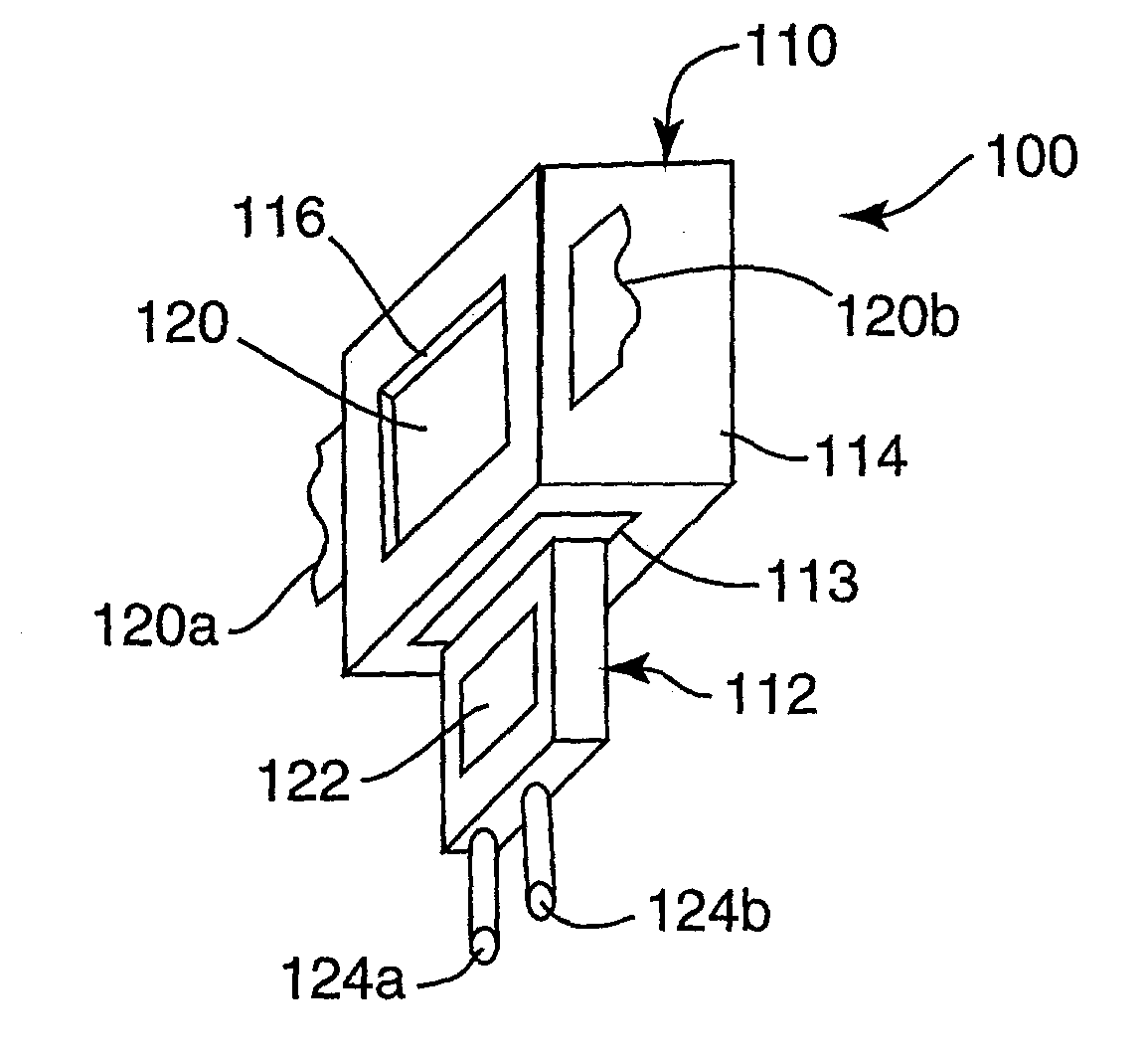
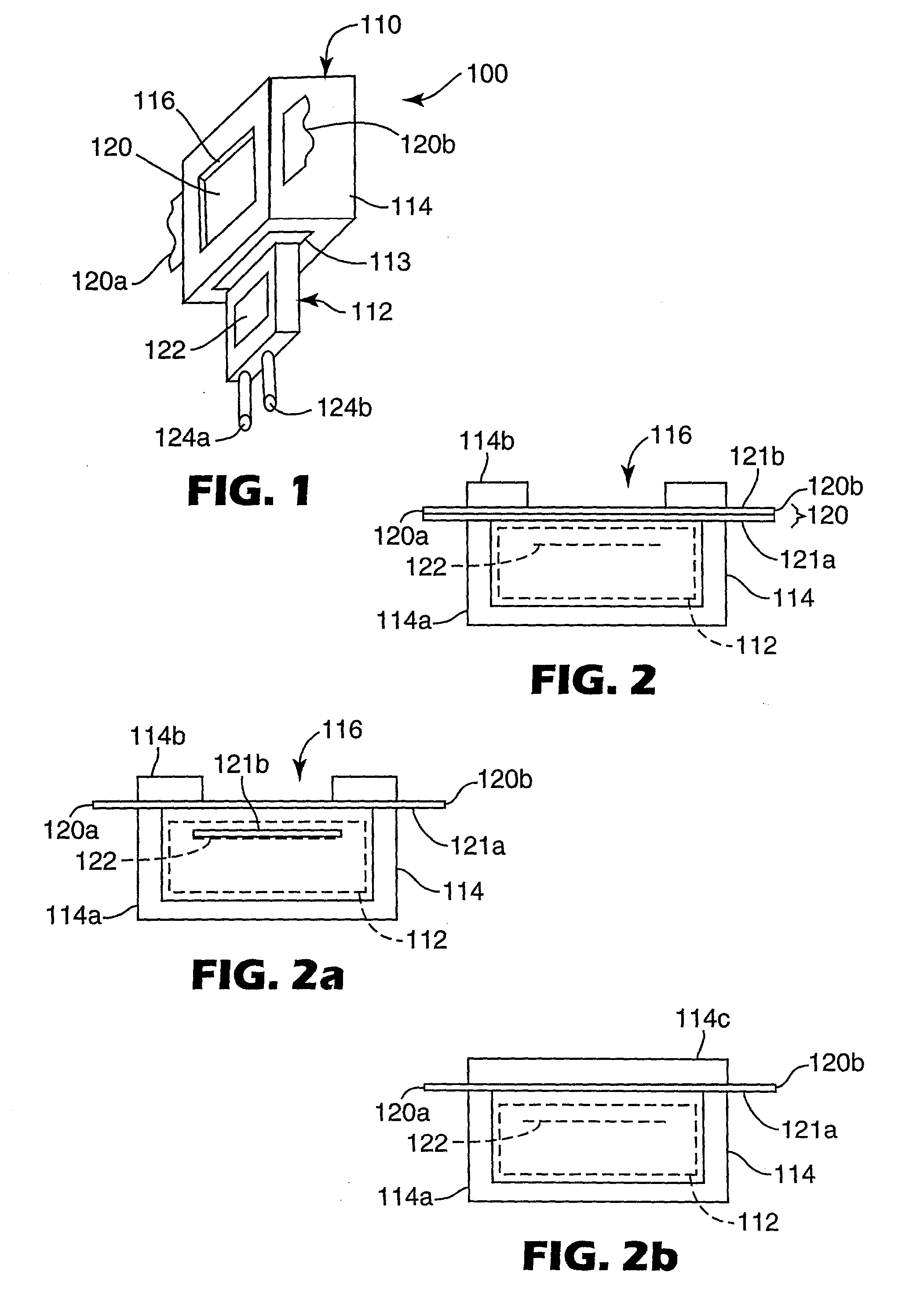
[0074] The interference element IF1 was laser cut to form strips using the procedure described in the U.S. Patent Application entitled "Method For Subdividing Multilayer Optical Film Cleanly and Rapidly" (Attorney Docket No. 57743US002) described above. Before removing the strips from the bottom liner, mixed ink composition GY2 was coated onto interference element IF1 using a spin coater, and organic solvent was evaporated in an oven at 80.degree. C. After drying, a polymer multilayer interference element having a 1.7 .mu.m thick green / yellow absorptive film thereon was obtained. This combination was further maintained in the oven at 70.degree. C. for 24 hours to promote crosslinking reaction. The green / yellow absorptive film had chromaticity values x=0.391, y=0.551. A strip of this combination was removed from the bottom liner, placed in an injection molding machine, and a box-type filter housing (see FIG. 1) was formed around the strip. The resulting filter assembly was placed ove...
example 3
[0075] The interference element IF1 was laser cut to form strips using the procedure described in the U.S. Patent Application entitled "Method For Subdividing Multilayer Optical Film Cleanly and Rapidly" (Attorney Docket No. 57743US002) described above. Before removing the strips from the bottom liner, mixed ink composition GY2 was coated onto interference element IF1 using a spin coater, and organic solvent was evaporated in an oven at 80.degree. C. After drying, a polymer multilayer interference element having a 1.7 .mu.m thick green / yellow absorptive film thereon was obtained. This combination was further maintained in the oven at 70.degree. C. for 24 hours to promote crosslinking reaction. The green / yellow absorptive film had chromaticity values x=0.391, y=0.551. A strip of this combination was removed from the bottom liner, placed in an injection molding machine, and a box-type filter housing (see FIG. 1) was formed around the strip. The resulting filter assembly was placed ove...
PUM
 Abstract
Description
Claims
Application Information


