Method of forming oxide layer using atomic layer deposition method and method of forming capacitor of semiconductor device using the same

a technology of atomic layer and forming method, which is applied in the direction of coating, transistor, chemical vapor deposition coating, etc., can solve the problems of gate penetration, gate leakage current increase, and threshold voltage reduction

Active Publication Date: 2004-02-19
SAMSUNG ELECTRONICS CO LTD
View PDF6 Cites 306 Cited by
  • Summary
  • Abstract
  • Description
  • Claims
  • Application Information

AI Technical Summary

Problems solved by technology

However, reducing the thickness of the gate insulation layer can result in several problems, such as increased gate leakage current, penetration of the gate by dopants or other impurities, reduced threshold voltages, etc.
When the cell capacitance decreases, the readability of data stored in the memory cell deteriorates, the likelihood of soft errors increases and the memory device becomes difficult to operate satisfactorily at low voltage.
However, when manufacturing a dynamic random access memory (DRAM) having a degree of integration necessary to achieve a capacity of about one gigabit or more, it is difficult to achieve a sufficiently high capac

Method used


Image

  • Method of forming oxide layer using atomic layer deposition method and method of forming capacitor of semiconductor device using the same
  • Method of forming oxide layer using atomic layer deposition method and method of forming capacitor of semiconductor device using the same
  • Method of forming oxide layer using atomic layer deposition method and method of forming capacitor of semiconductor device using the same

Examples


Embodiment Construction

[0043] Hereinafter, exemplary embodiments of the present invention will be described in detail.

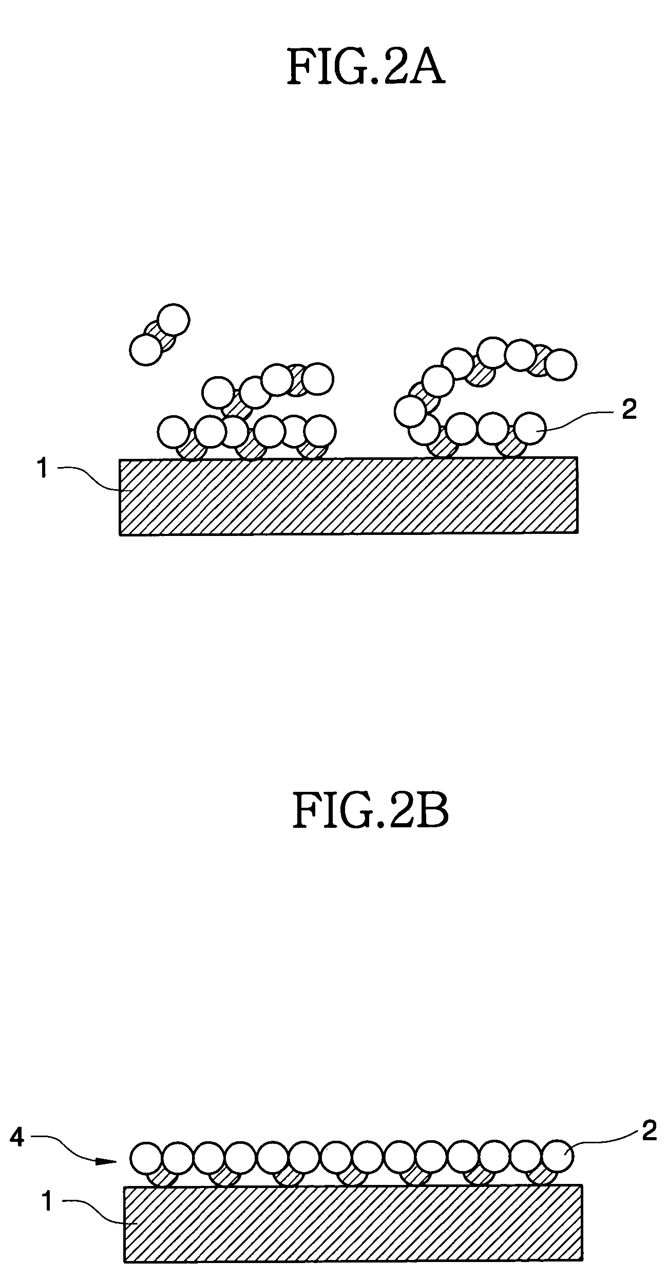
[0044] FIGS. 2A to 2E are cross-sectional views for explaining an exemplary embodiment of forming an oxide layer using an atomic layer deposition method. As illustrated in FIG. 2A, a substrate 1, such as a silicon wafer, is placed in a chamber in which a temperature of from about 100.degree. C. to about 500.degree. C. is maintained. The pressure of the chamber is controlled to about 0.4 Torr or less. In an exemplary embodiment, the temperature range is from about 150.degree. C. to about 350.degree. C. A precursor containing one central metal or semimetal element and an amino functional group is introduced into the chamber using an inert carrier gas such as argon (Ar) or nitrogen (N.sub.2) at a flow rate of about 50-5000 sccm for about 1-3 seconds to form an absorption layer 2 on the substrate. In an exemplary embodiment, the flow rate of the inert gas is in a range of about 500-1500 sccm.

[...


PUM

PropertyMeasurementUnit
Pressureaaaaaaaaaa
Angleaaaaaaaaaa
Currentaaaaaaaaaa

Abstract

In a method of forming an oxide layer using an atomic layer deposition and a method of forming a capacitor of a semiconductor device using the same, a precursor including an amino functional group is introduced onto a substrate to chemisorb a portion of the precursor on the substrate. Then, the non-chemisorbed precursor is removed. Thereafter, an oxidant is introduced onto the substrate to chemically react the chemisorbed precursor with the oxidant to form an oxide layer on the substrate. A deposition rate is fast and an oxide layer having a good deposition characteristic may be obtained. Also, a thin oxide film having a good step coverage and a decreased pattern loading rate can be formed.

Description

[0001] This application claims priority under 35 U.S.C. .sctn. 119 from Korean Patent Application No. 2002-48720, filed on Aug. 17, 2002, the contents of which are herein incorporated by reference in its entirety.[0002] 1. Field of the Invention[0003] The present invention relates to a method of forming an oxide layer and a method of forming a capacitor of a semiconductor device using such an oxide layer as the dielectric, and more particularly, to a method of forming an oxide layer using an atomic layer deposition (ALD) method and a method of forming a capacitor of a semiconductor device using the same.[0004] 2. Description of the Related Art[0005] As the demand for highly integrated semiconductor devices having high operating speeds has continued to increase, the surface area of the semiconductor substrate dedicated to each memory cell has been gradually reduced. As the area of the memory cells is reduced, the horizontal area available for forming the transistor(s) and / or capacito...

Claims


Application Information

Patent Timeline
IPC IPC(8): C23C16/40H01L21/205C23C16/44C23C16/455H01L21/02H01L21/316H01L21/8242H01L27/108
CPCC23C16/401C23C16/45553H01L21/02178H01L21/02181H01L21/022H01L21/0228H01L28/91H01L21/31604H01L21/3162H01L21/3165H01L21/31683H01L27/10817H01L27/10852H01L21/02304H10B12/318H10B12/033H01L21/205
Inventor LEE, YUN-JUNGPARK, IN-SUNGIM, GI-VINPARK, KI-YEONYEO, JAE-HYUN
Owner SAMSUNG ELECTRONICS CO LTD
Why Eureka
Try Eureka