High-frequency oscillator for an integrated semiconductor circuit and the use thereof

a technology of high-frequency oscillator and integrated semiconductor, which is applied in the direction of resonators, semiconductor devices, electrical equipment, etc., can solve the problems of ultrasonic units, relatively inconvenient use, and significant more precise laser distance measuring devices

Inactive Publication Date: 2004-03-11
ROBERT BOSCH GMBH
View PDF2 Cites 2 Cited by
  • Summary
  • Abstract
  • Description
  • Claims
  • Application Information

AI Technical Summary

Problems solved by technology

Ultrasonic units are very inexpensive, but are relatively imprecise for this task due to their low degree of beam focusing.
Laser distance measuring devices are significantly more precise, but cannot be miniaturized at will and are very expensive.
The sensors required for this are in fact based on semiconductor circuits, but the necessary excitation sources (oscillators) can only be installed into the semiconductor circuit later with conventional hybrid techniques.
It is disadvantageous here that the miniaturization is already limited due to the diffic

Method used


Image

  • High-frequency oscillator for an integrated semiconductor circuit and the use thereof
  • High-frequency oscillator for an integrated semiconductor circuit and the use thereof
  • High-frequency oscillator for an integrated semiconductor circuit and the use thereof

Examples


Embodiment Construction

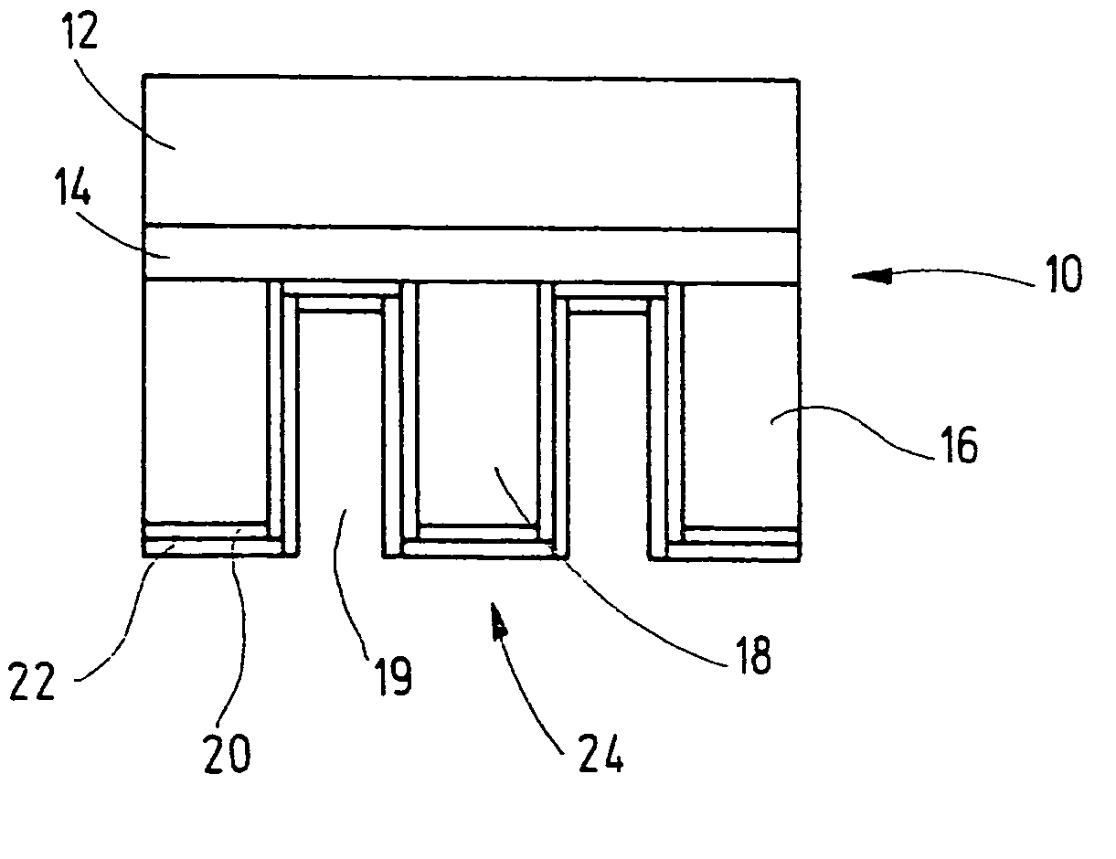
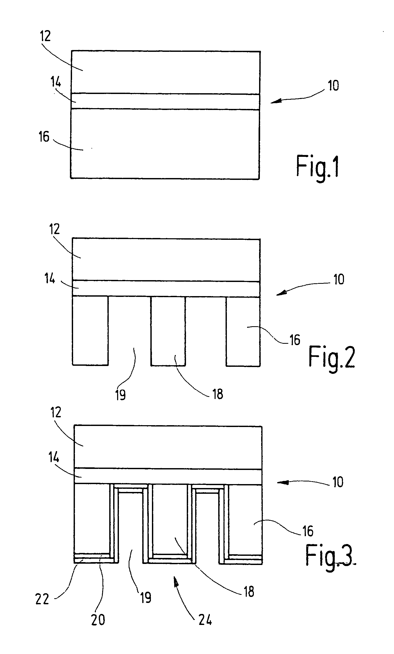
[0022] FIG. 1 shows a schematic sectional view of a detail from a conventional SOI (silicon on insulator) wafer that is used to produce a semiconductor circuit 10, which supports the high frequency oscillator 30 according to the invention. Because it is widely known, the known manufacture of all components of the semiconductor circuit 10 in a single manufacturing step using coplanar or planar techniques will not be explained in detail here. The wafer is comprised of a 675 .mu.m thick, semi-insulating p-doped structured layer 16 made of silicon. It has a specific resistance in the range from 500 to 1000 .OMEGA.cm, in particular 750 .OMEGA.cm. The structured layer 16 is coated with an approximately 300 nm thick insulation layer 14 of silicon dioxide, onto which is deposited a 50 .mu.m thick, p.sup.--doped layer 12 of silicon.

[0023] The insulation layer 14 of silicon dioxide serves as an etch stop in the trench etching of the micromechanical structures into the structured layer 16. The...


PUM


Abstract

The invention relates to a high frequency oscillator for an integrated semiconductor circuit and its use. The invention proposes that the high frequency oscillator (30) be a component of the semiconductor circuit (10), which is comprised of a first silicon layer (12), an adjoining silicon dioxide layer (insulation layer (14)), and an additional subsequent silicon layer (structured layer (16)), (SOI wafer), wherein the high frequency oscillator (30) is comprised of (a) a resonator (24) with a metallized cylinder (18) made of silicon disposed in the structured layer (16) and a coupling disk (28) that overlaps the cylinder (18) in the vicinity of the layer (12), and (b) an IMPATT diode (32) that is connected to the cylinder (18) of the resonator (24) via a recess (38) in the coupling disk (28).

Description

[0001] The invention relates to a high frequency oscillator for an integrated semiconductor circuit and use thereof.PRIOR ART[0002] The use of semiconductor technology in automotive engineering is on the rise. Miniaturization is permitting not only improved control and regulation techniques for engine-specific functions, but is also opening the way for new safety and driving comfort systems such as parking assistance, pre-crash and side-crash functions, blind spot detection, fill level measurements, and distance measurement. Sensory mechanisms in the vehicle--miniaturized if possible--must be provided for all controlling and regulating actions.[0003] As a rule, for the exemplary areas of used mentioned above, contactless sensors are used, which emit a measuring beam of a particular frequency that is reflected against the object to be measured, is received again by means of a receiver unit, and is then evaluated.[0004] For fill level measurements, there are known measuring devices in...

Claims


Application Information

Patent Timeline
IPC IPC(8): H01L21/84H01L27/04H01L21/822H01L27/12H01P7/06
CPCH01L21/84H01P7/065H01L27/1203H01P7/10
Inventor PFIZENMAIER, HEINZHASCH, JUERGEN
Owner ROBERT BOSCH GMBH
Why Eureka
Try Eureka