Slot fed microstrip antenna having enhanced slot electromagnetic coupling

a microstrip antenna and electromagnetic coupling technology, applied in the direction of antennas, antenna details, basic electric elements, etc., can solve the problems of inconvenient design of circuit components, and inability to meet the requirements of exceptionally high or low characteristic impedance values

Inactive Publication Date: 2004-08-26
HARRIS CORP
View PDF30 Cites 29 Cited by
  • Summary
  • Abstract
  • Description
  • Claims
  • Application Information

AI Technical Summary

Problems solved by technology

If the impedance of different parts of the circuit do not match, signal reflections and inefficient power transfer can result.
One problem encountered when designing microelectronic RF circuitry is the selection of a dielectric board substrate material that is reasonably suitable for all of the various passive components, radiating elements and transmission line circuits to be formed on the board.
Similarly, the line widths required for exceptionally high or low characteristic impedance values can, in many instances, be too narrow or too wide for practical implementation for a given substrate.
Still, an optimal board substrate material design choice for some components may be inconsistent with the optimal board substrate material for other components, such as antenna elements.
Moreover, some design objectives for a circuit component may be inconsistent with one another.
However, the use of a dielectric with a high dielectric constant will generally result in a significant reduction in the radiation efficiency of the antenna.
Dielectric loss is generally due to the imperfect behavior of bound charges, and exists whenever a dielectric material is placed in a time varying electromagnetic field.
Dielectric loss generally increases with operating frequency.
However, the use of a dielectric material having a low dielectric constant can present certain disadvantages, such as the large size of the slot antenna fabricated on a low dielectric constant substrate as compared to a slot antenna fabricated on a high dielectric constant

Method used


Image

  • Slot fed microstrip antenna having enhanced slot electromagnetic coupling
  • Slot fed microstrip antenna having enhanced slot electromagnetic coupling
  • Slot fed microstrip antenna having enhanced slot electromagnetic coupling

Examples


example 1

Slot with Air Above

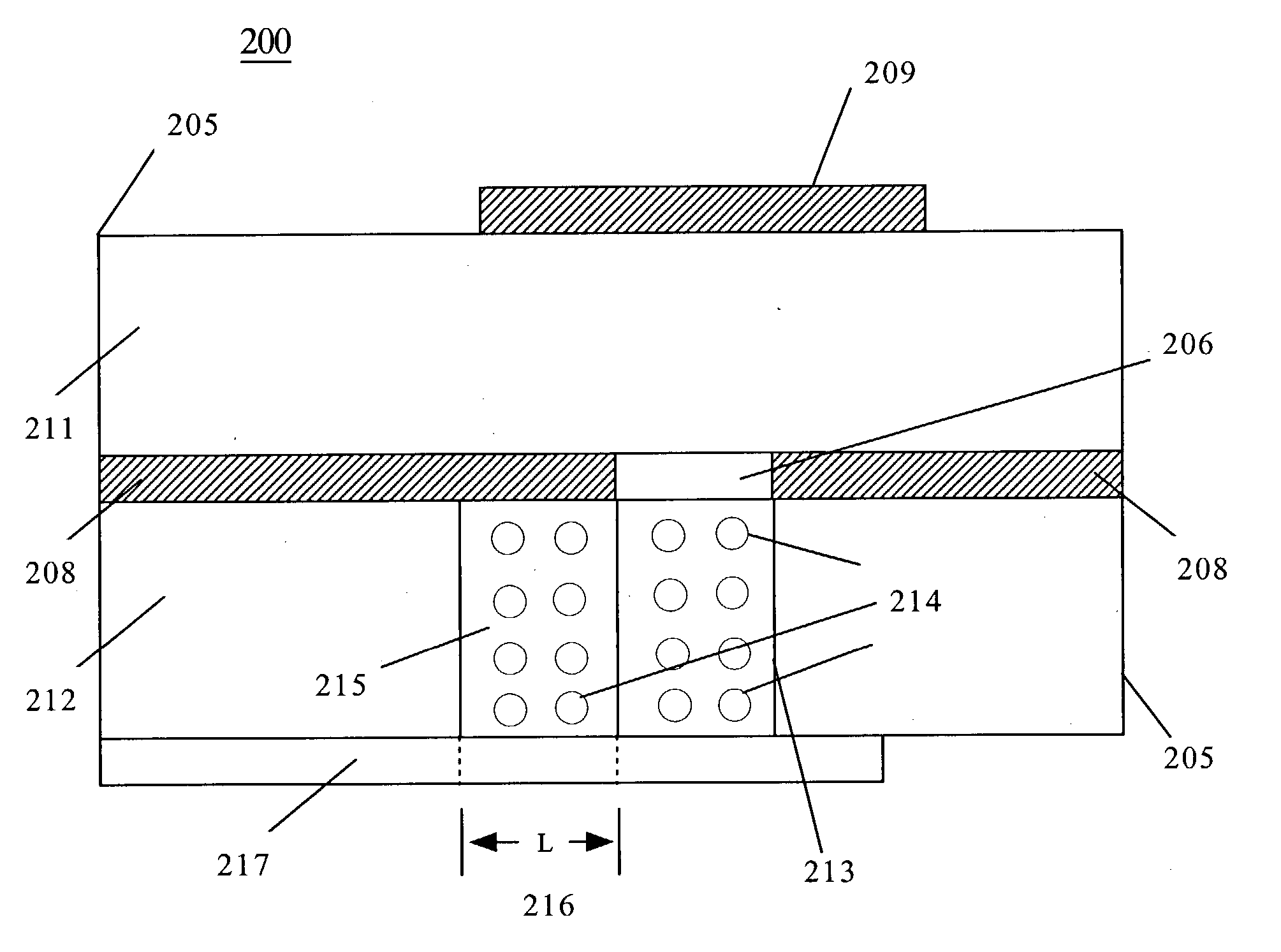
[0093] Referring to FIG. 5, a slot antenna 500 is shown having air (medium 1) above. Antenna 500 comprises transmission line 505 and ground plane 510, the ground plane including slot 515. A dielectric 530 having a dielectric constant .epsilon..sub.r=7.8 is disposed between transmission line 505 and ground plane 510 and comprises region / medium 4, region / medium 3 and region / medium 2. Region 3 has an associated length (L) which is indicated by reference 532. Region 525 is assumed to have little bearing on this analysis, and is thus neglected herein because it would add additional complexity not needed in order to explain the physical processes of interest.

[0094] The magnetic relative permeability values for medium 2 and 3 (.mu..sub.r.sub..sub.2 and .mu..sub.r.sub..sub.3) are determined by using the condition for the intrinsic impedance matching of mediums 2 and 3. Specifically, the relative permeability .mu..sub.r.sub..sub.2 of medium 2 is determined to permit the ma...

example 2

Slot with Dielectric Above, the Dielectric having a Relative Permeability of 1 and a Dielectric Constant of 10.

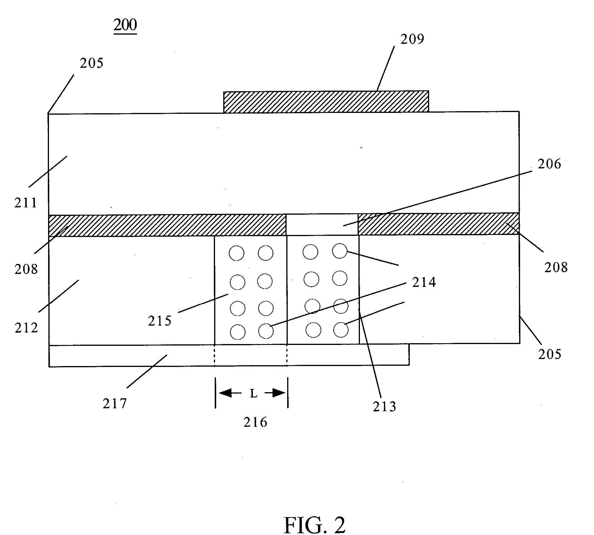
[0109] Referring to FIG. 6, a side view of a slot fed microstrip patch antenna 600 is shown formed on an antenna dielectric 610 which provides a dielectric constant .epsilon..sub.r=10 and a relative permeability .mu..sub.r=1. Antenna 600 includes the microstrip patch antenna 615 and the ground plane 620. The ground plane 620 includes a cutout region comprising a slot 625. The feed line dielectric 630 is disposed between ground plane 620 and microstrip feed line 640.

[0110] The feed line dielectric 630 comprises region / medium 4, region / medium 3 and region / medium 2. Region / medium 3 has an associated length (L) which is indicated by reference 632. Region 635 is assumed to have little bearing on this analysis and is thus neglected.

[0111] Since the relative permeability of the antenna dielectric is equal to 1 and the dielectric constant is 10, the antenna dielectric is clearly no...

example 3

Slot with Dielectric Above, That has a Relative Permeability of 10, and a Dielectric Constant of 20.

[0123] This example is analogous to example 2, having the structure shown in FIG. 6, except the dielectric constant .epsilon..sub.r of the antenna dielectric 610 is 20 instead of 1. Since the relative permeability of antenna dielectric 610 is equal to 10, and it is different from its relative permittivity, antenna dielectric 610 is again not matched to air. In this example, as in the previous example, the permeability for mediums 2 and 3 for optimum impedance matching between mediums 2 and 4 as well as for optimum impedance matching between mediums 1 and 2 are calculated. In addition, a length of the matching section in medium 3 is then determined which has a length of a quarter wavelength at a selected operating frequency. As before, the relative permeabilities .mu..sub.r.sub..sub.2, of medium 2 and .mu..sub.r.sub..sub.3 of medium 3, and the length L in medium 3 will be determined to...


PUM


Abstract

A slot fed microstrip antenna (100) provides improved efficiency through enhanced coupling of electromagnetic energy between the feed line (117) and the slot (106). The dielectric layer (105) between the feed line (117) and the slot (106) includes magnetic particles (114), the magnetic particles (114) preferably included in the dielectric junction region (113) between the microstrip feed line (117) and the slot (106). A high dielectric region is preferably also provided in the junction constant to further enhance the field concentration effect. The slot antenna (100) can be embodied as a microstrip patch antenna (200).

Description

STATEMENT OF THE TECHNICAL FIELD[0001] The inventive arrangements relate generally microstrip slot antennas.DESCRIPTION OF THE RELATED ART[0002] RF circuits, transmission lines and antenna elements are commonly manufactured on specially designed substrate boards. Conventional circuit board substrates are generally formed by processes such as casting or spray coating which generally result in uniform substrate physical properties, including the dielectric constant.[0003] For the purposes RF circuits, it is generally important to maintain careful control over impedance characteristics. If the impedance of different parts of the circuit do not match, signal reflections and inefficient power transfer can result. Electrical length of transmission lines and radiators in these circuits can also be a critical design factor.[0004] Two critical factors affecting circuit performance relate to the dielectric constant (sometimes referred to as the relative permittivity or .epsilon..sub.r) and th...

Claims


Application Information

Patent Timeline
IPC IPC(8): H01Q9/04
CPCH01Q9/0457
Inventor KILLEN, WILLIAM D.PIKE, RANDY T.
Owner HARRIS CORP
Why Eureka
Try Eureka