Beam Homogenizer, laser irradiation apparatus, and method of manufacturing a semiconductor device

a laser irradiation and semiconductor technology, applied in the direction of forging/pressing/hammering apparatus, handling devices, instruments, etc., can solve the problems of low quality of laser irradiation apparatus, poor homogeneity of beam spots on the surface to be irradiated,

Inactive Publication Date: 2004-09-16
SEMICON ENERGY LAB CO LTD
View PDF44 Cites 53 Cited by
  • Summary
  • Abstract
  • Description
  • Claims
  • Application Information

AI Technical Summary

Problems solved by technology

When the laser annealing is performed, however, there are some problems that a position of a plane having a homogeneous beam spot changes with the frequency of the pulsed excimer laser, that the homogeneity of the beam spot on the surface to

Method used


Image

  • Beam Homogenizer, laser irradiation apparatus, and method of manufacturing a semiconductor device
  • Beam Homogenizer, laser irradiation apparatus, and method of manufacturing a semiconductor device
  • Beam Homogenizer, laser irradiation apparatus, and method of manufacturing a semiconductor device

Examples


embodiment 1

[0070] [Embodiment 1]

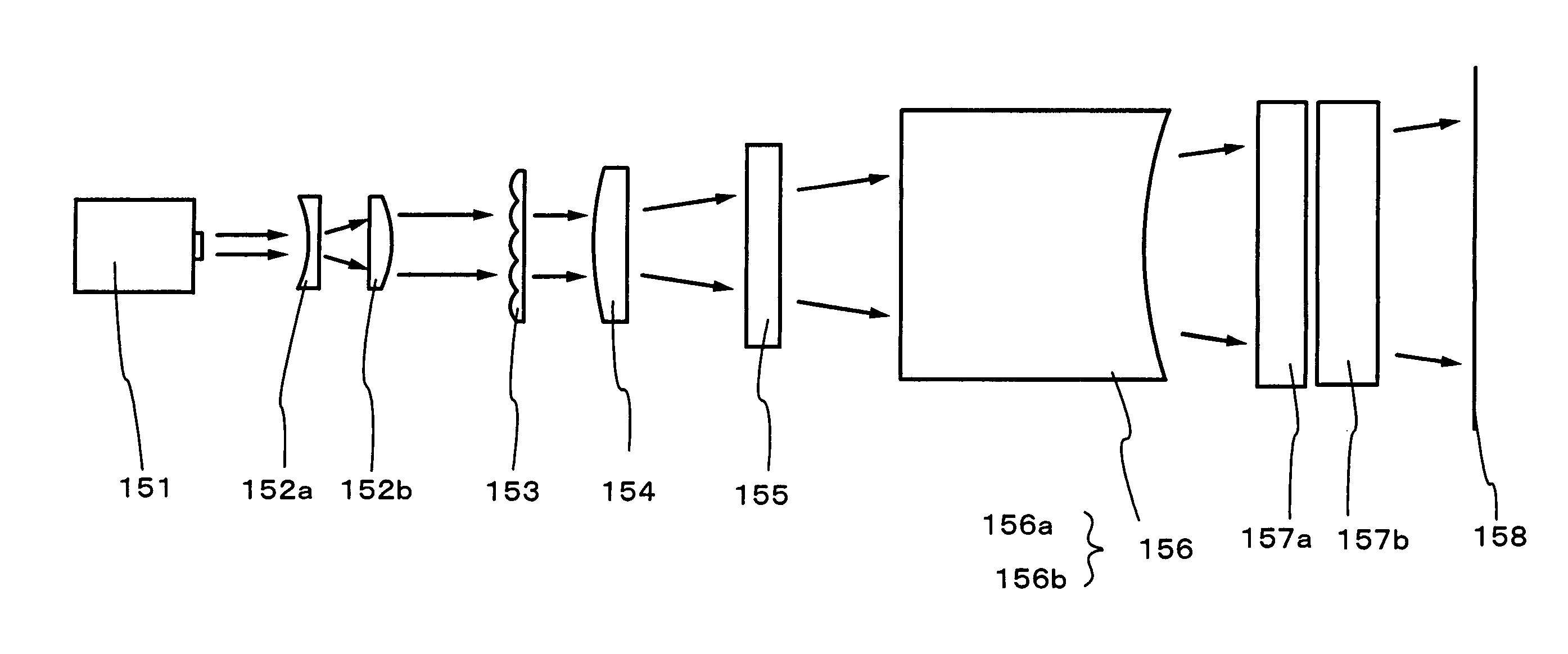
[0071] FIGS. 4A and 4B show an example of an optical system explained in this embodiment. First, a side view of FIG. 4B is explained. A laser beam emitted from a laser oscillator 151 is propagated to the direction indicated by an arrow in FIGS. 4A and 4B. The laser beam is expanded through spherical lenses 152a and 152b. This structure is not necessary when the beam spot emitted from the laser oscillator 151 is sufficiently large.

[0072] A cylindrical lens 155 having a thickness of 20 mm whose second surface has a radius of curvature of -194.25 mm is used to narrow the beam spot in the direction of the minor axis of the rectangular beam. The sign of the radius of curvature is positive when the center of the curvature is on the side where the beam is emitted with respect to the lens surface. The sign is negative when the center of the curvature is on the side where the beam is incident with respect to the lens surface. In addition, it is noted that a lens surface ...

embodiment 2

[0078] [Embodiment 2]

[0079] This embodiment exemplifies another optical system which is different from the optical system described in the embodiment mode. FIGS. 5A and 5B show the example of the optical system explained in this embodiment.

[0080] In FIGS. 5A and 5B, the laser beam goes through the same optical path as that shown in FIGS. 3A and 3B except for an optical waveguide 165. The optical waveguide 165 has a pair of reflection planes provided oppositely as well as the optical waveguide 135. The optical waveguide 135 has a hollow space between the pair of reflection planes. On the other hand, the optical waveguide 165 has the space filled with the medium 165c having a refractive index of "n". This is the different point between the two optical waveguides. In the case that the medium 165c has higher refractive index than the material of the reflection planes 165a and 165b, when the laser beam is incident into the optical waveguide 165 at an angle not more than the critical angl...

embodiment 3

[0083] [Embodiment 3]

[0084] In this embodiment, a process up to manufacture a semiconductor device with the crystalline semiconductor film by using the laser irradiation apparatus of the present invention is described with FIG. 8A-8D and FIG. 9A-9D.

[0085] First of all, base films 1101a and 1101b are formed on the substrate 1100. As the substrate 1100, an insulating substrate such as a glass substrate, a quartz substrate, or a crystalline glass substrate, or a ceramic substrate, a stainless substrate, a metal substrate (tantalum, tungsten, molybdenum, and the like), a semiconductor substrate, a plastic substrate (polyimide, acrylic, polyethylene terephthalate, polycarbonate, polyarylate, polyether sulfon and the like) can be used. It is noted that the substrate shall be made from the material that can resist the heat generated through the processes. A glass substrate is used in this embodiment.

[0086] As the base films 1101a and 1101b, a silicon oxide film, a silicon nitride film or a...


PUM

PropertyMeasurementUnit
Shapeaaaaaaaaaa
Distributionaaaaaaaaaa
Aspect ratioaaaaaaaaaa

Abstract

The present invention provides a beam homogenizer being equipped with an optical waveguide having a pair of reflection planes provided oppositely, having one end surface into which the laser beam is incident, and having the other end surface from which the laser beam is emitted in the optical system for forming the beam spot. The optical waveguide is a circuit being able to keep radiation light in a certain region and to transmit the radiation light in such a way that the energy flow thereof is guided in parallel with an axis of the channel.

Description

[0001] 1. Field of the Invention[0002] The present invention relates to a beam homogenizer to homogenize energy distribution of a beam spot on a surface to be irradiated in a certain region. The present invention also relates to a laser irradiation apparatus to irradiate the beam spot to the surface to be irradiated, and to a method for manufacturing a semiconductor device using the laser irradiation apparatus.[0003] 2. Description of the Related Art[0004] In recent years, the research has been conducted widely concerning the technique to perform laser annealing to an amorphous semiconductor film or a crystalline semiconductor film (a semiconductor film having a crystallinity such as poly-crystal or micro-crystal, which is not single-crystal) formed over an insulating substrate such as a glass substrate. A silicon film is often used as the semiconductor film. It is noted that the laser annealing described here indicates a technique to recrystallize a damaged layer or an amorphous la...

Claims


Application Information

Patent Timeline
IPC IPC(8): B23K26/00H01S5/10B23K26/06B23K26/073G02B27/09H01L21/3213H01L21/77H01L21/84
CPCB23K26/0639H01L27/1285B23K26/0648B23K26/0665B23K26/0732B23K2201/40G02B27/09G02B27/0911G02B27/0927G02B27/0966G02B27/0977G02B27/0994H01L21/02532H01L21/02678H01L21/02686H01L21/32136G02B19/0057G02B19/0095G02B19/0028B23K26/0643B23K26/064B23K2101/40B21K1/12B21J5/02B21J5/12B21K27/06
Inventor TANAKA, KOICHIRO
Owner SEMICON ENERGY LAB CO LTD
Why Eureka
Try Eureka