Thin film transistor substrate and method for manufacturing the same

Active Publication Date: 2004-10-07
HANNSTAR DISPLAY CORPORATION
View PDF11 Cites 19 Cited by
  • Summary
  • Abstract
  • Description
  • Claims
  • Application Information

AI Technical Summary

Problems solved by technology

However, the method disclosed in prior art 3 involves a problem in that an etching step of an insulating film which includes a photolithography step is additionally provided.
Thus, in the case where the respective steps are performed with insulating films (gate insulating films) that differ in thickness, it is difficult to achieve satisfactory circuit operation because it is difficult to match TFT characteristics, particularly, threshold voltages among plural kinds of TFTs.
In the impurity doping step, there arises a problem in that the number of photolithography steps and the number of impurity doping steps increase when impurities are doped in a self-aligning manner as to all the plural kinds of TFTs.
Further, when the thickness of the insulating film on the active layer exceeds 120 nm, there also arises a problem in that phosphorous is difficult to be doped because phosphorous is low insulating-film transmission capability.
However, in the case where the impurity is not doped in a self-aligning manner, an overlap or offset structure is invited by gate alignment, which leads to variation in t

Method used


Image

  • Thin film transistor substrate and method for manufacturing the same
  • Thin film transistor substrate and method for manufacturing the same
  • Thin film transistor substrate and method for manufacturing the same

Examples


first embodiment

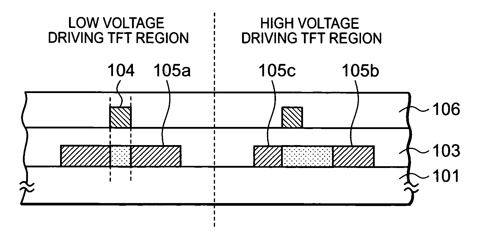
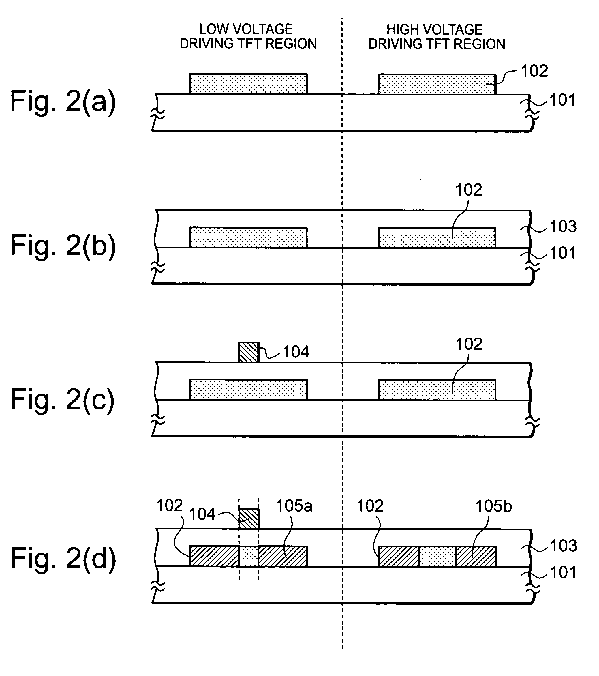
[0025] FIG. 2 and FIG. 3 are sectional views showing method steps according to the present invention. In the formation of a low voltage driving TFT and a high voltage driving TFT on an insulating substrate 101, at first, island-like active layers 102 are formed by patterning a poly-Si film formed by a laser annealing method (FIG. 2(a)). Next, an insulating film 103 is deposited (FIG. 2(b)). Here, the insulating film 103 serves as a gate insulating film of the low voltage driving TFT. Next, a first gate electrode 104 is formed (FIG. 2(c)). Here, it may be effective for lowering a TFT threshold voltage with high uniformity that the first gate electrode 104 takes a two-layer structure having a non-single crystal semiconductor for the lower layer, which is deposited by a plasma enhanced CVD method, and metal or metal silicide for the upper layer.

[0026] Next, impurities are doped into the island-like active layers 102, thereby forming impurity doping regions 105a (FIG. 2(d)). Here, in th...

second embodiment

[0035] FIGS. 4 and 5 are sectional views showing method steps according to a second embodiment of the present invention. The low voltage driving TFT has the same structure as that in the first embodiment. Thus, description thereof is appropriately omitted, and description will be made with respect to a high voltage driving TFT having a sub-gate structure. The sub-gate structure is excellent in output controllability at a low gate voltage, and therefore, is appropriate for a high withstand voltage TFT used for a level shift circuit.

[0036] The island-like active layers 102 are formed on a insulating substrate 101 with a laser annealing method. (FIG. 4(a)). Next, an insulating film 103 is deposited (FIG. 4(b). Subsequently, a first gate electrode 104 and a low voltage gate electrode 110 are formed (FIG. 4(c)). The two electrodes may be formed at the same time. Here, the first gate electrode 104 and the low voltage gate electrode 110 each may be formed as a two-layer structure for lower...

fourth embodiment

[0056] FIG. 9 shows the fifth example, wherein the sub-gate structure high voltage driving TFT 203 is formed as in the However, the drain is formed to have an LDD structure, and in addition, a low impurity concentration region 105f is formed in a channel region in a self-aligning manner with respect to the low voltage gate electrode 110. The low impurity concentration region 105f is formed of the same conductivity type and is at the same concentration as in the low impurity concentration region 105e, Here, the length of each of the low impurity concentration regions 105e and 105f is approximately 0.5 to 2 .mu.m.

[0057] FIG. 10 shows the sixth embodiment, wherein the drain is formed to have an LDD structure as in the fifth embodiment, and the low impurity concentration region 105f is formed in the channel region. The low impurity concentration region 105f is formed of the same conductivity type and is at the same concentration as in the low impurity concentration region 105e. Here, t...


PUM


Abstract

A thin film transistor substrate is provided including a first thin film transistor and a second thin film transistor. The first thin film transistor comprises a first active layer, a first gate insulating film, and a first gate electrode. The second thin film transistor comprises a second active layer formed, a second gate insulating film, and a second gate electrode. A thickness of the second gate insulating film is larger than a thickness of the first gate insulating film, the second active layer has at least two impurity doping regions which overlap the second gate electrode, the first active layer has at least two impurity doping regions formed in a self-aligning manner with respect to the first gate electrode, and the second gate electrode comprises a semiconductor layer.

Description

[0001] 1. Field of the Invention[0002] The present invention relates to a thin film transistor substrate and a method for manufacturing the same, and more particularly, to a thin film transistor substrate in which plural types of thin film transistors are formed on an insulating substrate, the plural types of transistors differing in driving voltage, for example, a driver circuit, a power source booster circuit, and a level shift circuit.[0003] 2. Description of the Related Art[0004] In recent years, by using polysilicon (poly-Si) thin film transistors (TFTs), pixel switch elements and also driver circuits can be formed on the same substrate in a liquid crystal device, organic EL display device, or the like which is formed on a low-cost glass substrate. A lower operation voltage is desired in the driver circuit for a lower power consumption. However, a voltage at some level or more is required in pixel operation. Therefore, there is required a technique in which plural types of TFTs...

Claims


Application Information

Patent Timeline
IPC IPC(8): H01L21/336H01L21/77H01L27/08H01L21/8234H01L21/84H01L27/088H01L27/12H01L29/423H01L29/786
CPCH01L27/1237H01L29/42384H01L27/124H01L29/78645H01L29/78624
Inventor OKUMURA, HIROSHI
Owner HANNSTAR DISPLAY CORPORATION
Why Eureka
Try Eureka