

Method for preparing nanocrystalline ceramic thin films
a nanocrystalline ceramic and thin film technology, applied in the direction of cell components, sustainable manufacturing/processing, final product manufacturing, etc., can solve the problems of difficult stabilization of microstructure in conventional production processes such as pressurized sintering and tape casting-sintering, and the scale application of these nanostructured materials. achieve the effect of cost efficien
- Summary
- Abstract
- Description
- Claims
- Application Information
AI Technical Summary
Benefits of technology
Problems solved by technology
Method used
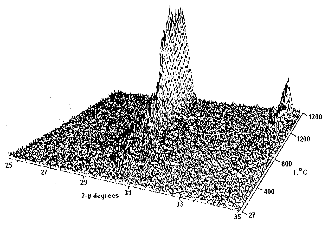
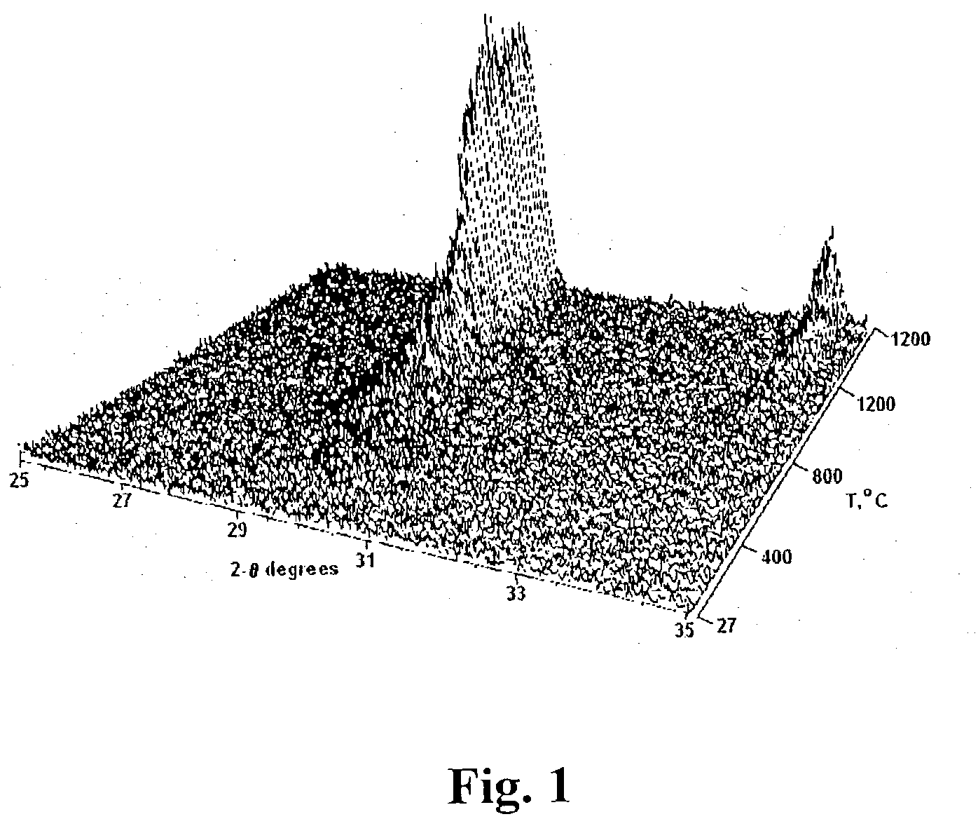
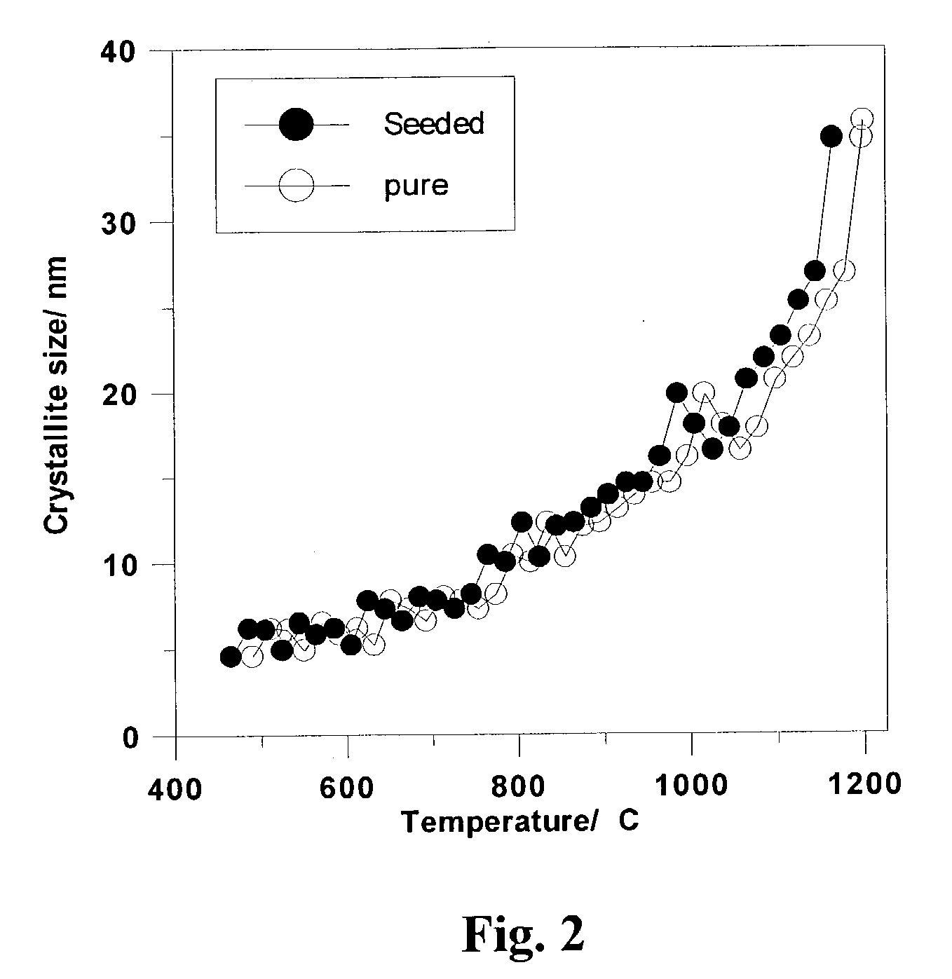
Image

Examples
example 1
[0024] Step 1. Preparation of seeded polymeric precursor. First, a zirconia sol-gel was prepared by adding 123 ml of zirconium n-propoxide (Alfa, Mw=327.56 g / mole, 70 purity, 0.25 mole=116.98 g 123 ml) into 500 ml of anhydrous isopropanol with stirring at room temperature and in water-free atmosphere (in nitrogen box). Then, the solution was added dropwise to 900 ml deionized water with stirring at 70.degree. C. and last 1-2 hours. A white sol-gel precipitate formed. Then, the solution was filtered with vacuum suction and the precipitate was washed in water several times. The product was diluted in 1 liter of water and peptized with 125 ml of 1 M HNO.sub.3 solution, followed by refluxing at 90.degree.-100.degree. C. over night with stirring. The sol-gel was re-dispersed in an ultrasonic bath for 30 minutes before use.
[0025] For making a precursor of YSZ with 16 mol % Y doping level: 20 ml of stable zirconia sol-gel (1.6 wt. % solid) was taken from the upper layer of the sol-gel, aft...
PUM
| Property | Measurement | Unit |
|---|---|---|
| thickness | aaaaa | aaaaa |
| temperature | aaaaa | aaaaa |
| temperatures | aaaaa | aaaaa |
Abstract
Description
Claims
Application Information