Strained-silicon-on-insulator single-and double-gate MOSFET and method for forming the same

a strain-silicon-on-insulator and mosfet technology, applied in the field of strain-silicon-on-insulator mosfet, can solve the problems of low efficiency of bulk devices, and low cost of bulk devices

Inactive Publication Date: 2004-12-16
IBM CORP
View PDF7 Cites 101 Cited by
  • Summary
  • Abstract
  • Description
  • Claims
  • Application Information

AI Technical Summary

Problems solved by technology

Another disadvantage is that a relatively thick (and thus relatively costly) SiGe epi-layer is needed.
Another disadvantage of the relaxed SiGe buffer layer technique is that it can only be used to make bulk devices.
Bulk devices do not have advantages such as the reduction in the junction capacitance and elimination of the latch-up path between devices, that are obtained by silicon-on-insulator (SOI) devices (e.g., see J-P.
While the wafer bonding technique discussed above may provide a way to obtain a strained-silicon layer on an insulator, it does not provide a method for straining the transferred silicon film, but relies on the conventional technique of growing the silicon film on a "plastically relaxed" SiGe layer.
The use of plastically relaxed SiGe as a template for growing strained silicon introduces problems such as large surface roughness and high defect concentration in the film.
1. Presently, bonding and layer transfer are expensive and are relatively low yield processes.
2. A long chemical mechanical polishing (CMP) step is typically required due to the SiGe layer roughness (e.g., topographical issues). The roughness is a result of the cross-hatch pattern that forms during the plastic relaxation of the SiGe layer.
3. The bonding strength may not be sufficient due to the use of a low bonding temperature. The lower bonding temperature is imposed to prevent Ge diffusion into silicon and to prevent relaxation of the strain silicon film.
4. A Smart-Cut.TM. process in which hydrogen is implanted into the SiGe buffer layer may be difficult to control since the hydrogen will partially relocate to defects in the SiGe film which are not at the intended blistering location.
First, it also uses wafer bonding to transfer the SiGe film, and therefore has some of the problems discussed earlier.
Second, the anneal at the BPSG reflow temperature leads to diffusion of boron and phosphorus from the glass into the SiGe film. This is an undesirable effect since both boron and phosphorus are dopants of silicon and SiGe.
Third, some of the strain in the film relaxes by buckling of the SiGe film. This leads to an undulated rough surface.

Method used


Image

  • Strained-silicon-on-insulator single-and double-gate MOSFET and method for forming the same
  • Strained-silicon-on-insulator single-and double-gate MOSFET and method for forming the same
  • Strained-silicon-on-insulator single-and double-gate MOSFET and method for forming the same

Examples


second embodiment

[0103] Second Embodiment

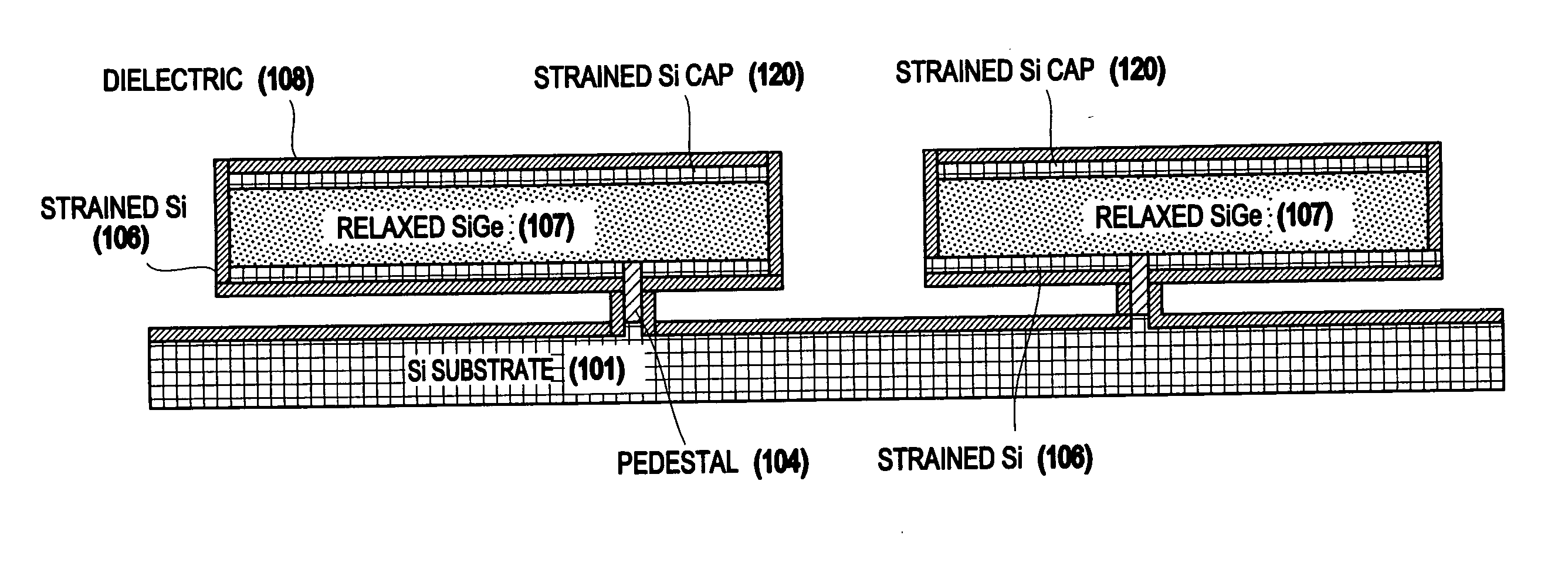
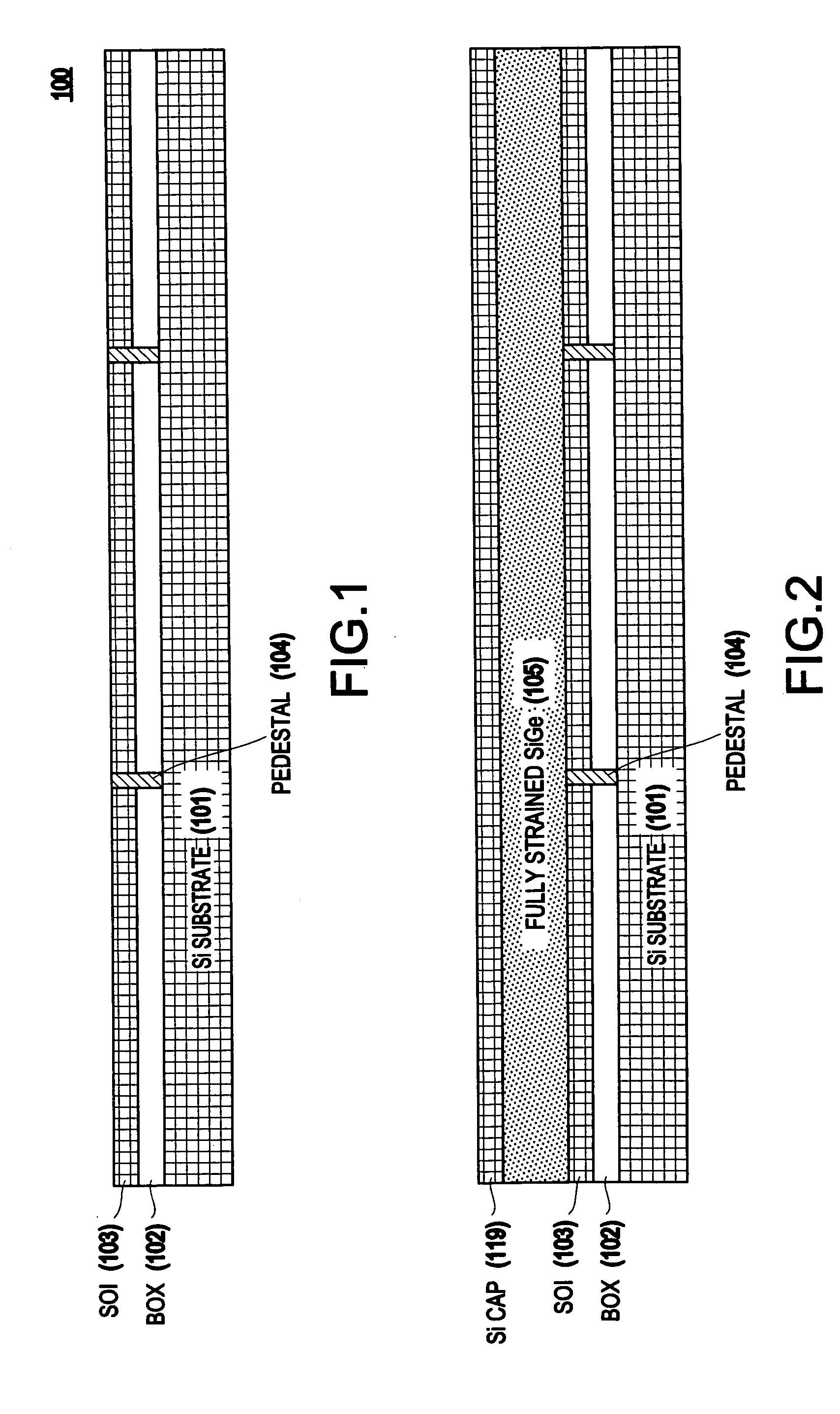
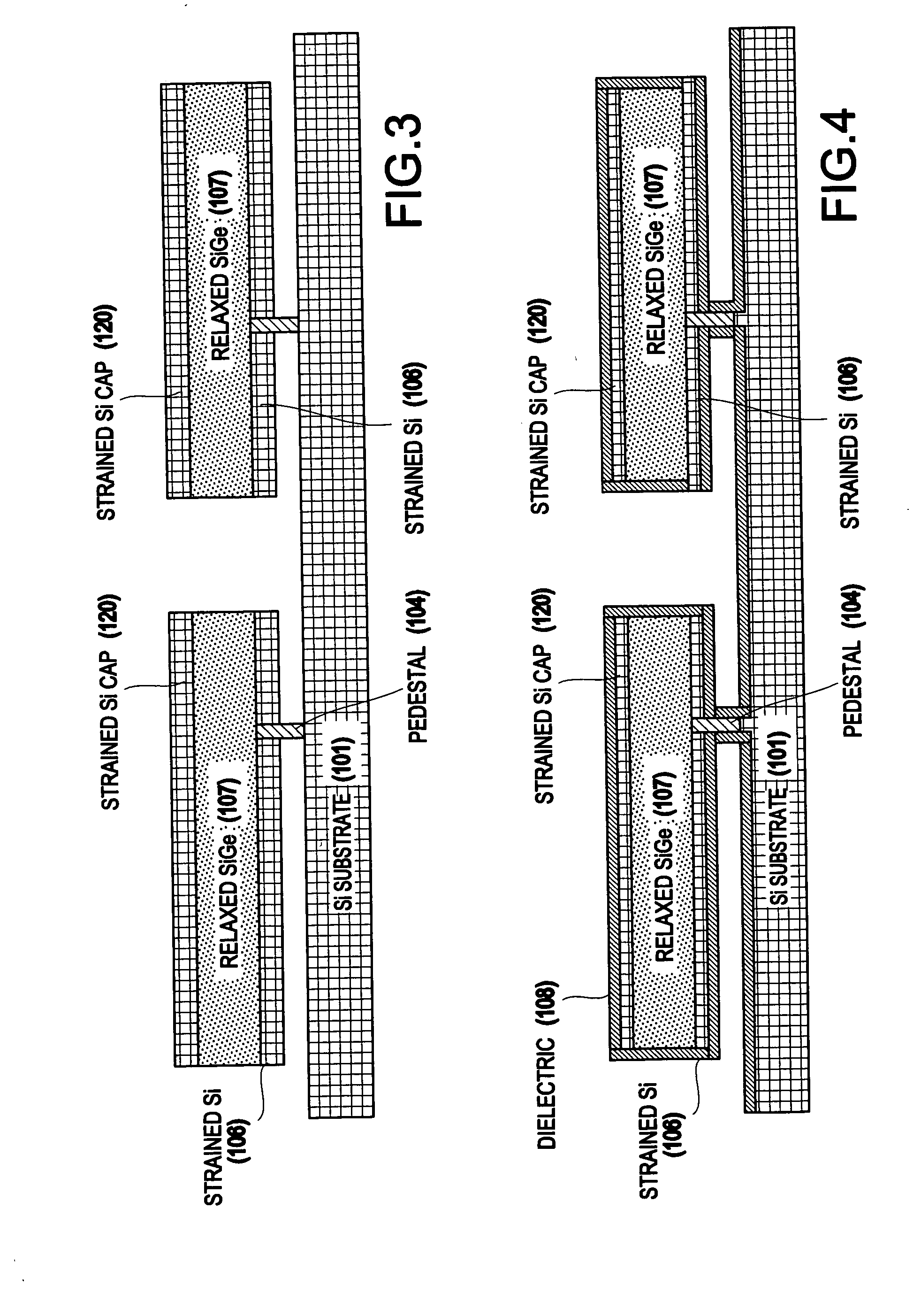
[0104] Turning now to FIG. 11 and to a different structure, it is noted that bowing occurs since the free-standing structure includes a bilayer of two mismatched materials such as SiGe over silicon. The bowing can be prevented by sandwiching the SiGe 107 film between two silicon films (106 and 120) of equal thicknesses, as was discussed above and shown in FIGS. 2-6. The sandwiched SiGe film 107 does not bow since the silicon layer 106 balances the silicon cap layer 120.

[0105] Hence, whereas before in FIGS. 2-6, a sandwich layer was shown of relaxed SiGe with strained silicon on first and second sides (e.g., top and bottom), in FIGS. 11-12, a first side (e.g., the top) of the strained silicon has been removed.

[0106] However, the use of a cap layer 120 decreases the degree of strain relaxation in SiGe film 107, since the total silicon film thickness, t.sub.Si, is twice as thick compared with a bilayer structure (e.g., SiGe over silicon without a silicon cap).

[0...

third embodiment

[0110] Third Embodiment

[0111] It is noted that the fabrication of a free-standing structure according to the present invention does not necessarily require the use of a SOI wafer, but can also be achieved with a bulk silicon wafer as the starting wafer. This allows the integration of mixed complementary metal oxide semiconductor (CMOS) technologies (e.g., bulk Si CMOS with SSOI CMOS, etc.).

[0112] Referring now to FIGS. 13-20, a bulk silicon substrate 121 is implanted with a p-type dopant such as boron. The implant forms a buried p-doped layer 122 which is capped by an undoped silicon layer 123, as shown in FIG. 13. Alternatively, the p-doped layer 22 can be realized by in-situ doped epitaxial growth of p-type silicon followed by an epitaxial growth of undoped silicon to form the cap layer 123.

[0113] The pedestal location is defined by a masked implant that forms a localized pillar of doped silicon 122A. The structure is then annealed to activate the dopants. The pedestal can also be...

fourth embodiment

[0123] Fourth Embodiment

[0124] FIGS. 21-25 describe an embodiment in which a free-standing silicon film 136 is strained by the deposition of a straining material 137. It is assumed in this embodiment a BOX 132 and SOI 133 is used. Of course, a bulk silicon substrate could be used instead, as demonstrated above.

[0125] As shown in FIGS. 21-22, a free-standing silicon film 136 is formed by first forming a pedestal 134, patterning the SOI film 133, and etching the BOX 132.

[0126] Then, as shown in FIG. 23, a straining material 137 is deposited over the free-standing silicon and over the silicon substrate 131.

[0127] An exemplary feature of this embodiment is that the straining material can be many materials (e.g., SiGe, or a material other than SiGe such as a layer of silicon nitride, etc.). Hence, the straining material 37 can be deposited as single-crystal by epitaxy, or it can be deposited as an amorphous or poly-crystalline material. Examples of single-crystal materials are SiGe, SiC ...


PUM


Abstract

A method of forming a semiconductor structure (and the resulting structure), includes straining a free-standing semiconductor, and fixing the strained, free-standing semiconductor to a substrate.

Description

[0001] 1. Field of the Invention[0002] The present invention relates to a semiconductor device, and more particularly to a strained-silicon-on insulator MOSFET with a single or a double gate, and to a method of forming a strained-silicon-on-insulator structure.[0003] 2. Description of the Related Art[0004] A MOSFET fabricated in 001-oriented silicon under biaxial tensile strain exhibits higher carrier mobilities than a conventional MOSFET (e.g., see K. Rim, J. L. Hoyt, J. F. Gibbons, "Fabrication and Analysis of Deep Submicron Strained-Si N-MOSFET's", EEE Trans. Electron Devices, 47(7), p. 1406, (2000)). The higher carrier mobility leads to a higher current drive and thus a faster / shorter switching time is obtained.[0005] The "strained" silicon film is typically formed by growing an epitaxial silicon layer on top of a strain-relaxed, graded SiGe layer structure (e.g., see P. M. Mooney, Materials Science and Engineering Reports R17, p. 105 (1996) and references therein).[0006] As kno...

Claims


Application Information

Patent Timeline
Patent Type & Authority Applications(United States)
IPC IPC(8): H01L21/762H01L21/8238H01L21/84
CPCH01L21/76264H01L21/823807H01L21/84H01L27/1203H01L29/7842
Inventor COHEN, GUY MOSHEMOONEY, PATRICIA MAY
Owner IBM CORP
Why Eureka
Try Eureka