Lithographic apparatus, device manufacturing method and device manufacturing thereby

a technology of lithographic apparatus and manufacturing method, applied in the direction of photomechanical exposure apparatus, printers, instruments, etc., can solve the problems of inability to achieve absolute accuracy and in particular thermal stability over long travel ranges, and inability to meet the requirements of high-speed printing

Inactive Publication Date: 2004-12-30
ASML NETHERLANDS BV
View PDF36 Cites 231 Cited by
  • Summary
  • Abstract
  • Description
  • Claims
  • Application Information

AI Technical Summary

Benefits of technology

[0042] a displacement measuring system for measuring the position of a moveable object comprising one of said support structure and said substrate table in at least two degrees of freedom, said displacement measuring system comprising at least one grid grating mounted on a reference frame and at least one sensor head mounted on said moveable object for measuring displacement of said moveable object relative to said grid grating in two degrees of freedom. A major advantage of the 2D grid encoder is that the measurement grid can be permanently fixed on a grating plate. Even if the grating is not perfectly orthogonal, straight or linear, this remains unchanged as long as the grating plate is free from distortions (either thermal or elastic). Such linearity or orthogonality errors can be calibrated out without too much difficulty by, for example, vacuum interferometry. The calibration only needs to be performed once for each grating, or not at all if one is only interested in positional repeatability. The use of a grid encoder essentially removes the guideway straightness and orthogonality from the error budget, when compared with single-axis encoder-based solutions.
[0049] Capacitive sensors, on the other hand, can be designed as an absolute sensor with very high stability. Furthermore, the distance measurement is performed over a relatively large target surface, which helps to reduce any effects of localized unevenness of the target surface. Despite their limited measurement range and stand-off clearance, they are currently the preferred choice in lithographic applications.
[0050] An encoder based nano-positioning system offers an advantageous alternative to interferometry and is much simpler to implement. Better measurement stability can be achieved by the fact that the measurement grid in the X-Y plane is permanently fixed onto the mask table, which when implemented in a zero-CTE material, such as Zerodur, is both long-term dimensionally stable and thermally insensitive. This eases considerably the stringent demand on environmental control of the area immediately around the optical path of the interferometer beams, particularly in the case of a lithographic projection apparatus employing wavelengths of 157 nm or below. Such devices require to be purged with gas, that does not absorb the beam (which is strongly absorbed in air), and by avoiding the need for air showers over the length of the interferometer beams, the present invention can substantially reduce consumption of purge gas.
[0057] In the lithographic projection system according to the invention, the number of interferometers used for measuring the displacements of the substrate table relative to the projection system is reduced. This way, the costs of both the measurement system and the substrate table are reduced.

Problems solved by technology

One of the most challenging requirements for micro-lithography for the production of integrated circuits as well as liquid crystal display panels is the positioning of tables.
Although such sensors can provide sub-micrometer level resolution without difficulty, absolute accuracy and in particular thermal stability over long travel ranges are not readily achievable.
Although the technology behind such interferometer systems is very mature, their application is not without problems.
One of the most significant drawbacks of the interferometer is the dependence of wavelength on environmental pressure and temperature, as described by Schellekens P. H J.
This remains one of the major problems in the thermal design of an optical lithography system.
In addition, the mounting adjustment of multi-axis interferometers for orthogonality and coplanarity, as well as the subsequent calibration procedure to remove any residual errors, are both extremely complex and time consuming.
Furthermore, the pointing stability of the laser beam during operation may introduce additional cosine or Abbe errors which need to be calibrated out on a regular basis by some form of automated routine.
Although metrology frames in state-of-the-art lithography systems are highly isolated from ambient vibration, thermal deformation of the order of 0.5.times.10.sup.-9 m is not totally avoidable.
Mounting of interferometers directly on the lens, for example, is both difficult and undesirable.
Relative length measurement to the lens can, however, still be realized by differential interferometry, at the expense of the added complication and cost.
The multiple beams required for such 6 DOF interferometric measurement cannot be adequately supplied with sufficient optical power by one laser source, thus requiring multiple sources with additional wavelength matching demands.
As can be seen, whilst the resulting interferometry based system is technically viable and has been implemented in practice, it is by no means simple, robust and economical.
As such, they do not lend themselves readily to nano-metrology in all 6 DOF simultaneously.
Amongst the difficulties is the high level of crosstalk of the displacement signal to parasitic movements in the other 5 DOF.
The use of inductive sensors against a Zerodur chuck is problematic, as conductive targets are required for the sensors.
Pneumatic proximity sensors (air micrometer), on the other hand, suffer from limited resolution and working distance, as well as exerting a finite force on the target.
As an absolute sensor, however, they do suffer from long-term stability problems due to mechanical drifts (thermal or otherwise) requiring periodic calibration.

Method used


Image

  • Lithographic apparatus, device manufacturing method and device manufacturing thereby
  • Lithographic apparatus, device manufacturing method and device manufacturing thereby
  • Lithographic apparatus, device manufacturing method and device manufacturing thereby

Examples


Embodiment Construction

1

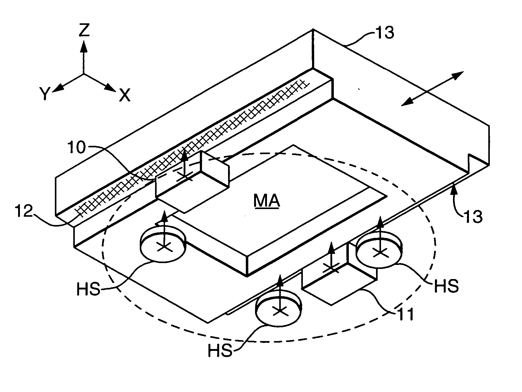
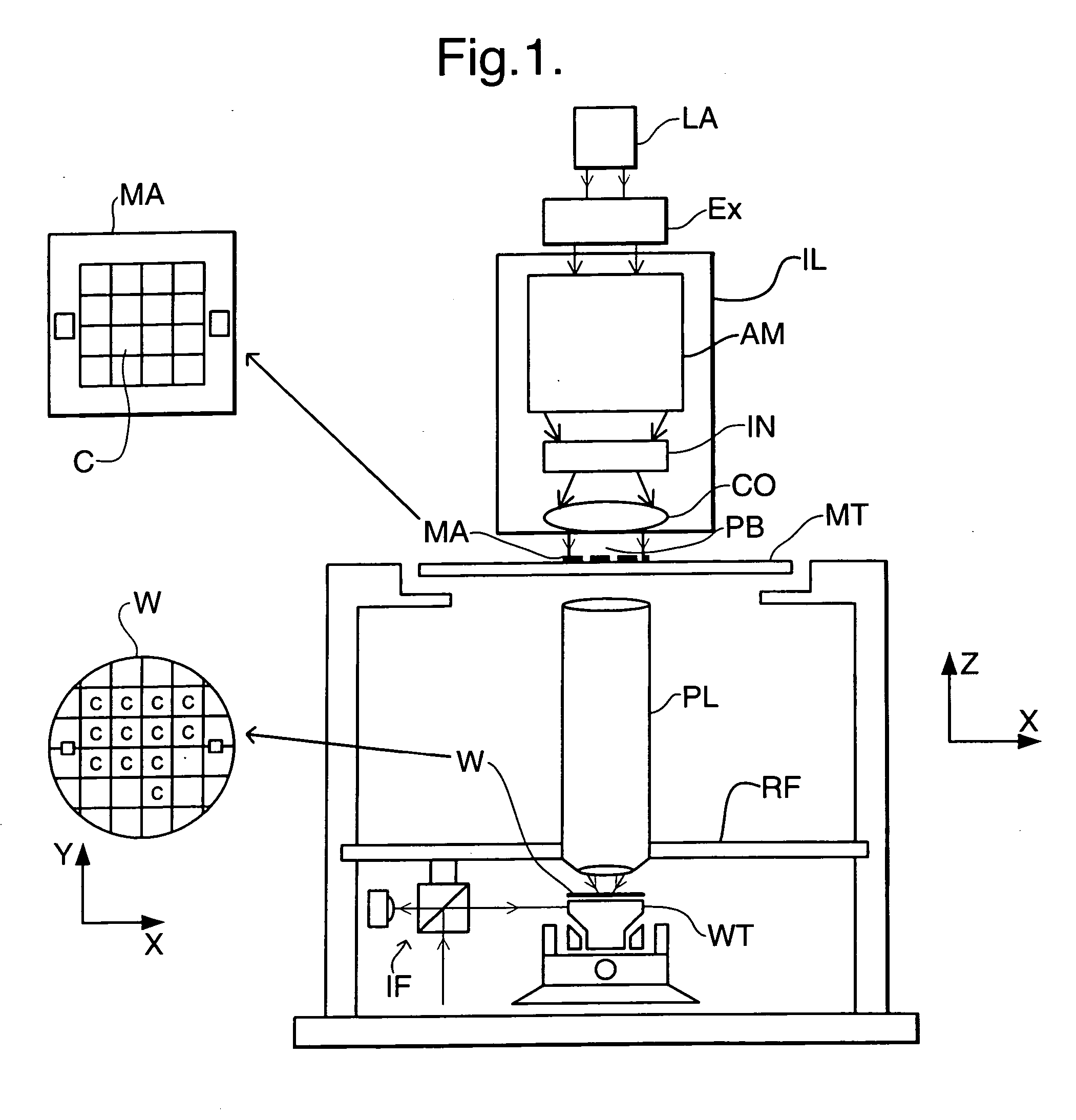
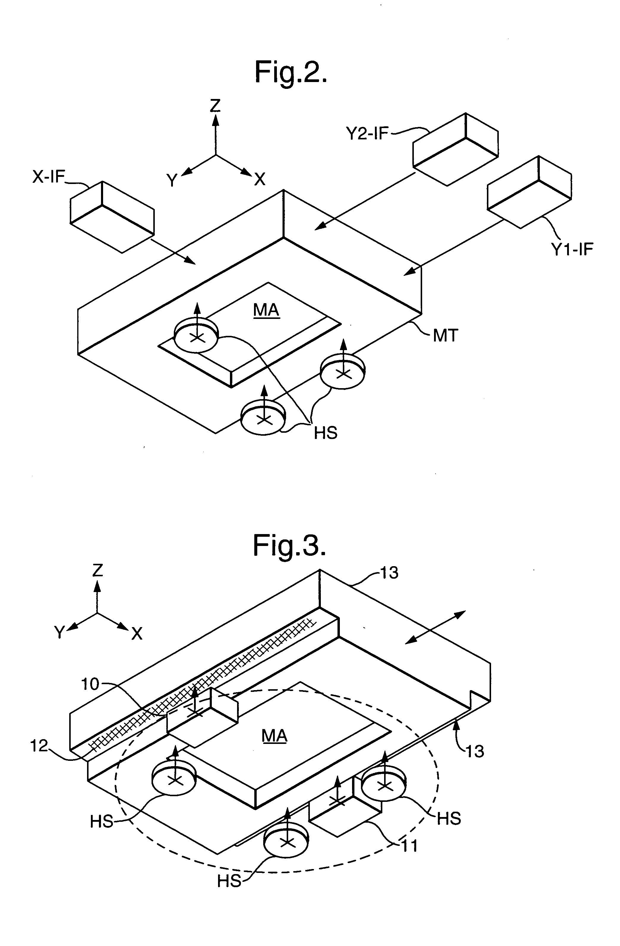
[0083] FIG. 1 schematically depicts a lithographic projection apparatus according to a particular embodiment of the invention. The apparatus comprises:

[0084] a radiation system Ex, IL, for supplying a projection beam PB of radiation (e.g. UV radiation), which in this particular case also comprises a radiation source LA;

[0085] a first object table (mask table) MT provided with a mask holder for holding a mask MA (e.g. a reticle), and connected to first positioning module for accurately positioning the mask with respect to item PL;

[0086] a second object table (substrate table) WT provided with a substrate holder for holding a substrate W (e.g. a resist-coated silicon wafer), and connected to second positioning module for accurately positioning the substrate with respect to item PL;

[0087] a projection system ("lens") PL (e.g. lens group) for imaging an irradiated portion of the mask MA onto a target portion C (e.g. comprising one or more dies) of the substrate W. As here depicted, the...


PUM

PropertyMeasurementUnit
degrees of freedomaaaaaaaaaa
wavelengthsaaaaaaaaaa
wavelengthaaaaaaaaaa

Abstract

The X, Y and Rx positions of a mask stage are measured using two optical encoder-reading heads measuring displacements of respective grid gratings mounted on the mask stage. The grid gratings are preferably provided on cut-away portions of the mask table so as to be coplanar with the pattern on the mask itself. Measurements of the table position in the other degrees of freedom can be measured with capacitative or optical height sensors.

Description

[0001] This application is a continuation-in-part application of U.S. patent application Ser. No. 09 / 928,462, filed Aug. 22, 2001, which claims priority to EP 00307306.1 filed Aug. 24, 2000, the contents of which are incorporated herein by reference in their entirety.[0002] 1. Field of the Invention[0003] The present invention relates generally to lithographic projection apparatus.[0004] 2. Description of the Prior Art[0005] The term "patterning device" as here employed should be broadly interpreted as referring to devices that can be used to endow an incoming radiation beam with a patterned cross-section, corresponding to a pattern that is to be created in a target portion of the substrate; the term "light valve" can also be used in this context. Generally, the pattern will correspond to a particular functional layer in a device being created in the target portion, such as an integrated circuit or other device (see below). Examples of such patterning devices include:[0006] A mask. ...

Claims


Application Information

Patent Timeline
Patent Type & Authority Applications(United States)
IPC IPC(8): G03F7/20G03F9/00
CPCG03F7/70716G03F7/70725G03F9/7053
Inventor KWAN, YIM BUN PATRICK
Owner ASML NETHERLANDS BV
Why Eureka
Try Eureka