

Method of machining semiconductor wafer-use polishing pad and semiconductor wafer-use polishing pad
a technology of polishing pad and semiconductor wafer, which is applied in the direction of manufacturing tools, grinding devices, other chemical processes, etc., can solve the problems of increasing the surface roughness of the inner surface of the groove, the difficulty of cutting in the depth direction of the groove, and the inability to form a lattice-like groove with high dimensional accuracy in width and depth from time to tim
- Summary
- Abstract
- Description
- Claims
- Application Information
AI Technical Summary
Benefits of technology
Problems solved by technology
Method used
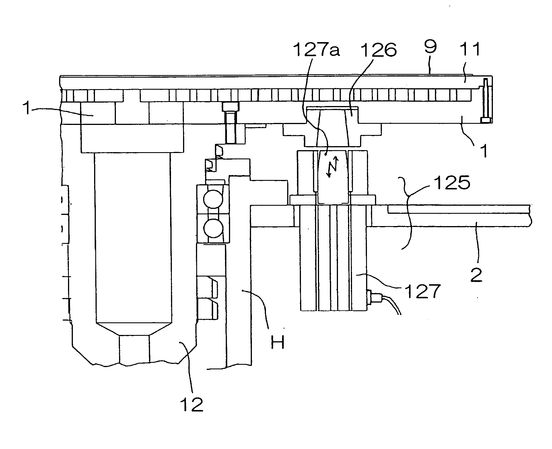
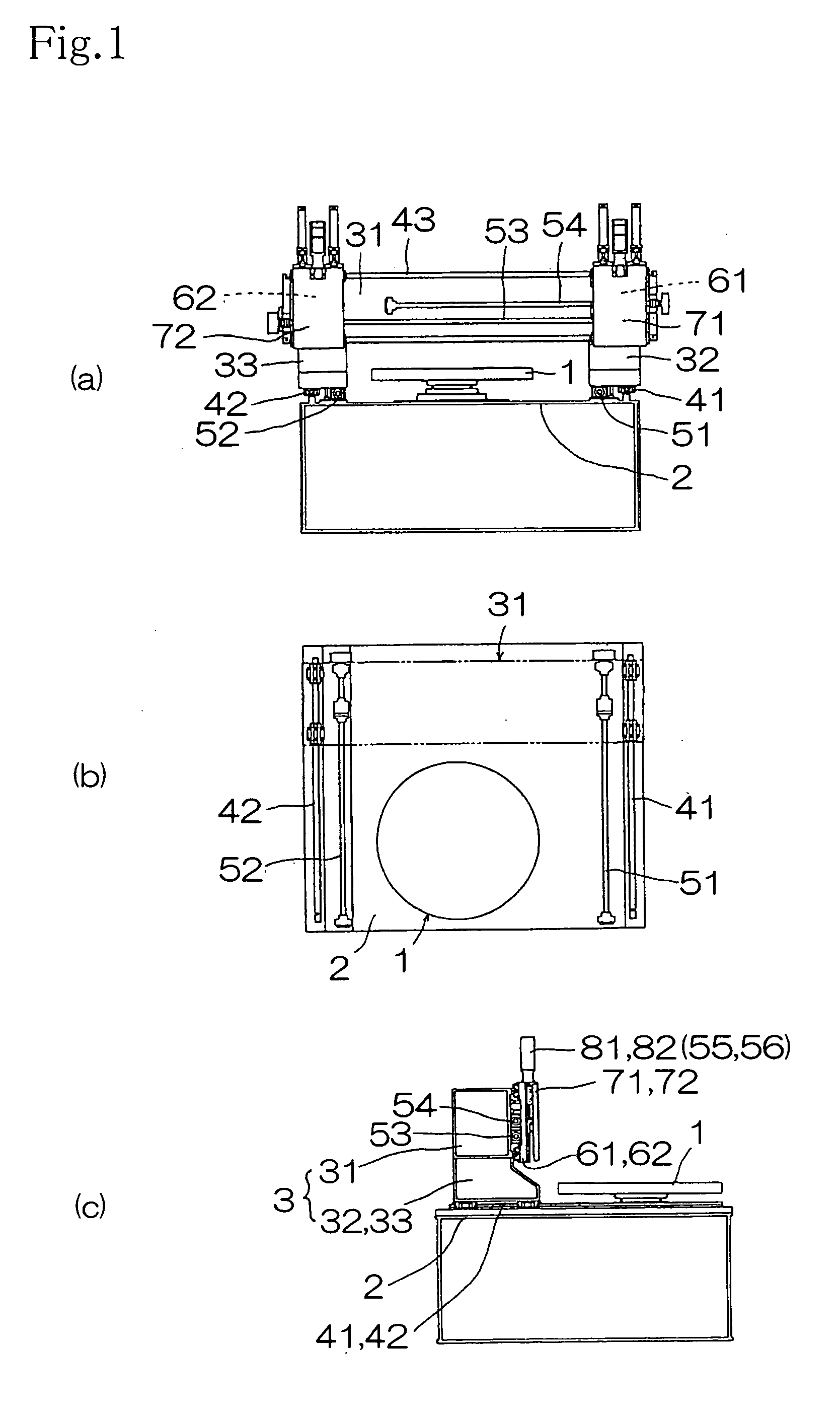
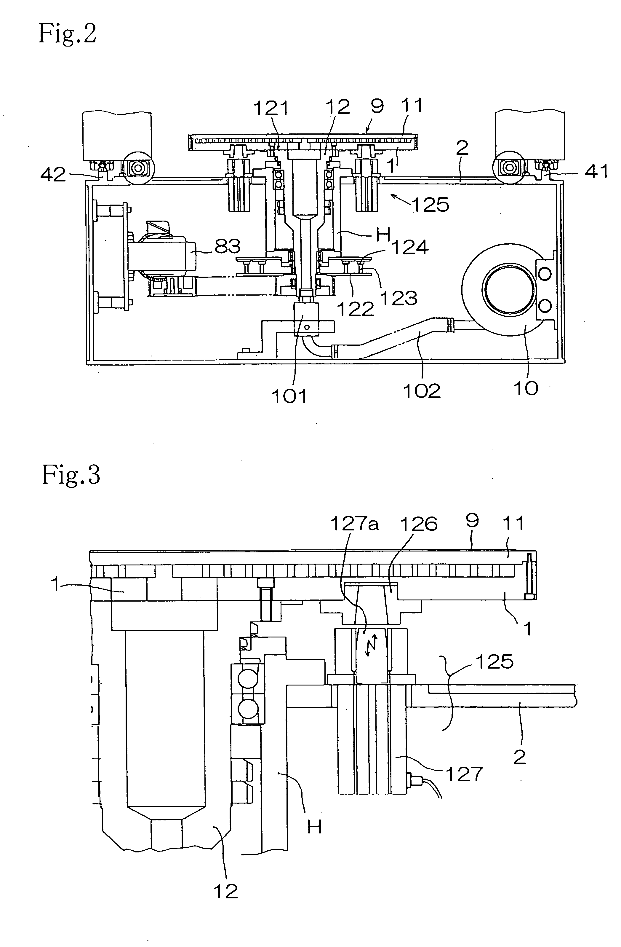
Image

Examples
example 1
[0162] 70 parts by mass of non-crosslinked 1,2-polybutadiene (Trade name "JSR RB830" manufactured by JSR Corp.), 30 parts by mass of non-crosslinked ethylene-vinyl acetate copolymer (Trade name, "Ultrathene 630" manufactured by Tosoh Corp.), and 40 parts by mass of .beta.-cyclodextrin (Trade name "Dexipearl .beta.-100" manufactured by Bio Research Corporation of Yokohama, having average particle diameter of 20 .mu.m) as a water-soluble particle were kneaded with the use of a biaxial extruder controlled at a temperature of 160.degree. C. Subsequently, 1.0 part by mass of an organic peroxide (Trade name "Percumyl D-40" manufactured by NOF Corp.) was added and further kneaded, and the mixed product was extruded into a mold. After that, it underwent a crosslinking process of holding it at a temperature of 170.degree. C. for 18 minutes, obtaining a polishing pad, 60 cm in diameter and 3 mm in thickness. Then, plural annular grooves were formed concentrically on the polishing surface of t...
example 2
[0177] A polishing pad having the same size was produced similarly to Example 1, and plural annular grooves were formed concentrically on the polishing surface of the polishing pad according to the method described in [2], where the average value of the groove width was 0.5 mm, the average value of the groove depth was 1 mm, and the average value of the pitch was 1 mm.
[0178] The surface roughness of the inner surface of the groove was 5.2 .mu.m, and variations in the surface roughness were also small. Additionally, the dimensional accuracy was .+-.4% in width, .+-.5% in depth, and .+-.5% in pitch, being excellent. Furthermore, a removal rate, an existence of scratches and a dishing were evaluated similarly to Example 1. As the result, the removal rate was 300 nm / min, scratches were hardly observed, and dishing was 60 nm; the polished surface was excellent in flatness.
example 3
[0179] 80 parts by mass of non-crosslinked ethylene-vinyl acetate copolymer (Trade name, "Ultrathene 630" manufactured by Tosoh Corp.), 20 parts by mass of non-crosslinked 1,2-polybutadiene (made by JSR Corporation, product name, JSR RB830), and 100 parts by mass of .beta.-cyclodextrin (Trade name "Dexipearl .beta.-100" manufactured by Bio Research Corporation of Yokohama, having average particle diameter of 20 .mu.m) as a water-soluble particle were kneaded with the use of a biaxial extruder controlled at a temperature of 160.degree. C. Subsequently, 0.5 parts by mass of an organic peroxide (Trade name "Percumyl D-40" manufactured by NOF Corp.) was added and further kneaded, and the mixed product was extruded into a mold controlled at a temperature of 170.degree. C. It underwent a crosslinking process of holding it at a temperature of 170.degree. C. for 18 minutes, obtaining a polishing pad, 60 cm in diameter and 3 mm in thickness. Then, plural annular grooves were formed concentri...
PUM
| Property | Measurement | Unit |
|---|---|---|
| Fraction | aaaaa | aaaaa |
| Angle | aaaaa | aaaaa |
| Angle | aaaaa | aaaaa |
Abstract
Description
Claims
Application Information