Semiconductor memory device including an SOI substrate

a memory device and soi technology, applied in the direction of solid-state devices, transistors, instruments, etc., can solve the problems of data inversion, leakage current flow between the source and the drain, and the reduction of the gate length, so as to achieve stable operation

Inactive Publication Date: 2005-01-06
RENESAS ELECTRONICS CORP
View PDF20 Cites 9 Cited by
  • Summary
  • Abstract
  • Description
  • Claims
  • Application Information

AI Technical Summary

Benefits of technology

[0016] Still another object of the present invention is to further increase the data retaining time in a memory cell.
[0053] Because the body region of an N channel MOS transistor that is not directly connected to a ground node is fixed, the threshold voltage of the transistor including that fixed body region is reduced, whereby the transistor operates more speedily. Therefore, those transistor can operate properly even when the power supply voltage is low.

Problems solved by technology

This change in the amount of charge will result in data inversion, i.e., soft error.
Although the gate length is generally reduced to increase the integration density of a DRAM, this reduction in gate length has a limitation due to a significant short channel effect as the channel length is reduced.
There is also a possibility of a leakage current flow between the source and the drain.
Therefore, the transistor cannot operate stably.

Method used


Image

  • Semiconductor memory device including an SOI substrate
  • Semiconductor memory device including an SOI substrate
  • Semiconductor memory device including an SOI substrate

Examples


embodiment 1

[0117] Embodiment 1

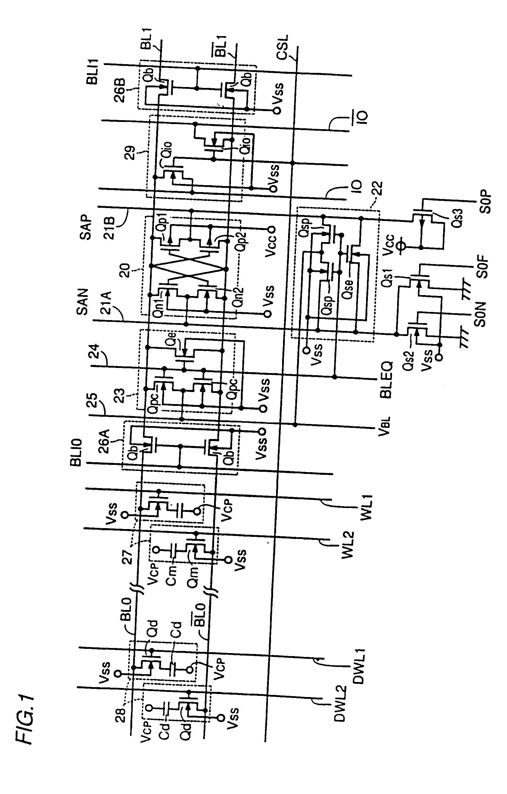
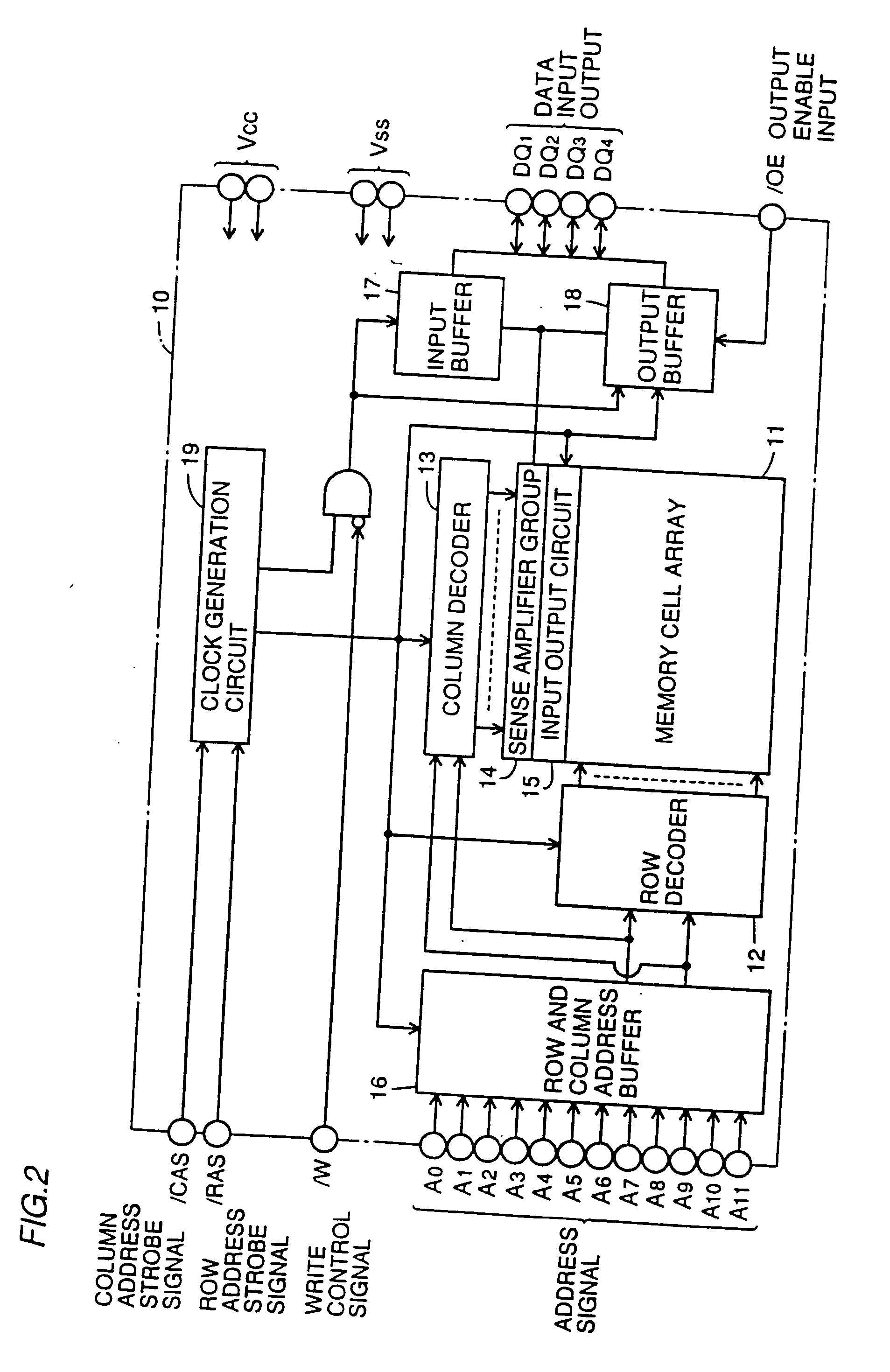
[0118]FIG. 2 is a block diagram showing an entire structure of a DRAM according to embodiment 1 of the present invention. Referring to FIG. 2, a DRAM 10 includes a memory cell array 11, a row decoder 12, a column decoder 13, a sense amplifier group 14, an input / output circuit 15, a row-and-column address buffer 16, an input buffer 17, an output buffer 18, and a clock generation circuit 19.

[0119] In memory cell array 11, a plurality of word lines (not shown) are disposed along the row direction, and a plurality of bit line pairs (not shown) are disposed along the column direction, with a plurality of memory cells (not shown) at the crossings thereof. Row decoder 12 responds to a row address signal from address buffer 16 to select and drive one of the plurality of word lines. Column decoder 13 responds to a column address signal from address buffer 16 to select one of the plurality of bit line pairs. Sense amplifier group 14 includes a plurality of sense amplifiers...

embodiment 2

[0167] Embodiment 2

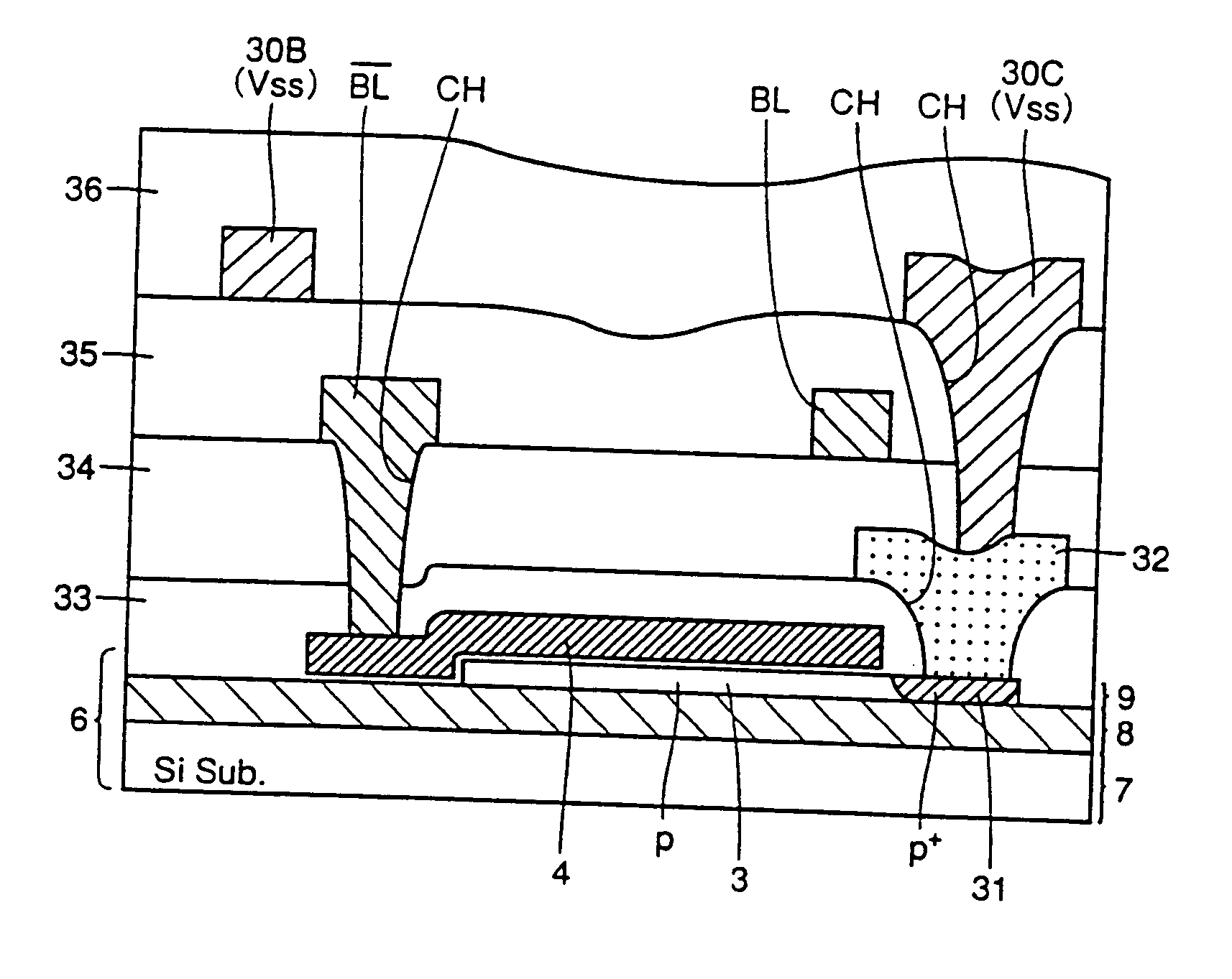
[0168]FIG. 8 is a plan view showing a structure of sense amplifier 20 partially and precharge circuit 23 entirely in a DRAM according to embodiment 2 of the present invention.

[0169] Referring to FIG. 8-, embodiment 2 has both body regions 3 protruding in the same direction with a contact region 31 formed at that protruding portion. Both contact regions 31 are connected to one body fix line 30C via respective contact holes CH. Also, both gate electrodes 4 protrude in the same direction. The protruding portions thereof are connected to bit lines BL1 and / BL1 via respective contact holes CH.

[0170] Embodiment 2 has a layout area smaller than that of embodiment 1 since body fix line 30C for fixing body regions 3 of transistors Qn1 and Qn2 are common.

embodiment 3

[0171] Embodiment 3

[0172]FIG. 9 is a plan view showing a structure of sense amplifier 20 partially and precharge circuit 23 entirely of a DRAM according to embodiment 3 of the present invention. Referring to FIG. 9, precharge circuit 23 differs from the precharge circuit of embodiment 1 in that it is disposed in a 180° rotated position. Body regions 3 of transistors Qe and Qpc in precharge circuit 23 are connected to body fix line 30B via contact region 31 and contact hole CH. Body region 3 of transistor Qn2 of sense amplifier 20 is also connected to body fix line 30B via contact region 31 and contact hole CH.

[0173] Embodiment 3 has a layout area smaller than that of embodiment 1 since body fix line 30B for fixing body region 3 of transistor Qn2 of sense amplifier 20 is common to the body fix line for fixing body region 3 of transistors Qe and Qpc in precharge circuit 23.


PUM


Abstract

A semiconductor memory device includes a plurality of N and P channel MOS transistors. The plurality of MOS transistors are formed on an SOI (Silicon On Insulator) substrate. Each MOS transistor includes a source region, a drain region, and a body region located between the source region and the drain region. The body region of at least one N channel MOS transistor is electrically fixed. The body region of at least one P channel MOS transistor is rendered floating.

Description

BACKGROUND OF THE INVENTION [0001] 1. Field of the Invention [0002] The present invention relates to semiconductor memory devices, and more particularly to a dynamic random access memory (DRAM) formed on an SOI (Silicon On Insulator) substrate. [0003] 2. Description of the Background Art [0004] A semiconductor memory device is typically divided into a volatile memory such as a RAM, and a non-volatile memory such as a ROM. The volatile memory is further divided into a DRAM and a static random access memory (SRAM). The non-volatile memory includes a mask ROM, an EPROM, a flash memory, an EEPROM, a fuse ROM, and the like. [0005] A DRAM has data stored by accumulating charge in the capacitor of a memory cell. Although such a DRAM requires a refresh operation, a DRAM having a large storage capacity can be manufactured at a low cost due to its simple structure of the memory cell. [0006] Because data is stored by accumulating charge in a capacitor in a DRAM, the amount of charge stored in ...

Claims


Application Information

Patent Timeline
Patent Type & Authority Applications(United States)
IPC IPC(8): G11C5/02G11C11/401H01L21/316G11C11/407G11C11/408H01L21/762H01L21/8242H01L27/10H01L27/108H01L27/12H01L29/78H01L29/786
CPCG11C11/404G11C11/4097G11C2211/4016H01L21/84H01L27/1203H01L27/108H01L27/10802H01L27/10897H01L27/0207H10B12/20H10B12/00H10B12/50
Inventor HIDAKA, HIDETOSUMA, KATSUHIROTSURUDA, TAKAHIRO
Owner RENESAS ELECTRONICS CORP
Why Eureka
Try Eureka