
Selective etching of silicon carbide films

a technology of silicon carbide and selective etching, which is applied in the direction of acceleration measurement using interia forces, instruments, coatings, etc., can solve the problems of poor control of lateral dimensions, special equipment, and difficult wet etching of si

Active Publication Date: 2005-01-06
RGT UNIV OF CALIFORNIA
View PDF8 Cites 246 Cited by
  • Summary
  • Abstract
  • Description
  • Claims
  • Application Information

AI Technical Summary

Problems solved by technology

One of the challenges in fabricating SiC devices is related to the selective etching of SiC films or SiC bulk materials.
Unlike silicon (“Si”), SiC is not etched significantly by most acids and bases at temperatures less than 600° C., which makes wet etching of SiC a difficult task to accomplish.
Non-standard techniques such as laser-assisted photoelectrochemical etching of SiC have been developed, but they require special equipment and have poor control over the lateral dimensions.
However, metal masks in RIE are known to cause micromasking phenomena, where metal atoms of the mask material are sputtered by the plasma and deposited in the etch field, producing grass-like structures, which are undesirable.
In addition, metal masks in RIE result in contamination of the substrate in subsequent fabrication steps, as well as the microfabrication tools, and hence, are commonly prohibited in integrated circuit (IC) processing.

Method used


Image

  • Selective etching of silicon carbide films
  • Selective etching of silicon carbide films
  • Selective etching of silicon carbide films

Examples


Embodiment Construction

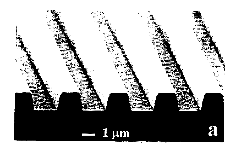
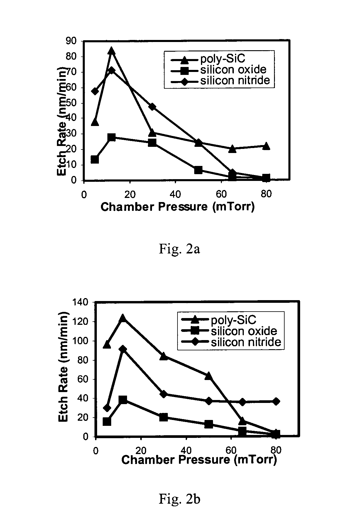
[0016] Embodiments of the present invention are directed towards methods for etching SiC with a highly selective RIE process using a non-metallic mask layer. In certain embodiments, instead of using fluorinated gases, etching is performed using a hydrogen and bromine etch chemistry. This allows the use of non-metallic material such as silicon dioxide to mask a SiC substrate during the etch. In one aspect, the etching is performed using a hydrogen bromide (“HBr”) etch chemistry in a plasma chamber. An HBr etch chemistry has been used to etch silicon, but not silicon dioxide, silicon nitride or SiC. Conventional wisdom of those skilled in the art would teach away from using HBr to etch SiC, since SiC is a very stable material. In addition, it is generally expected that silicon dioxide or silicon nitride would etch at a faster rate than SiC. Because of this, HBr would not ordinarily be considered as an effective etchant against a stable material such as SiC. The present invention, howe...


PUM

PropertyMeasurementUnit
Poweraaaaaaaaaa
Poweraaaaaaaaaa
Poweraaaaaaaaaa

Abstract

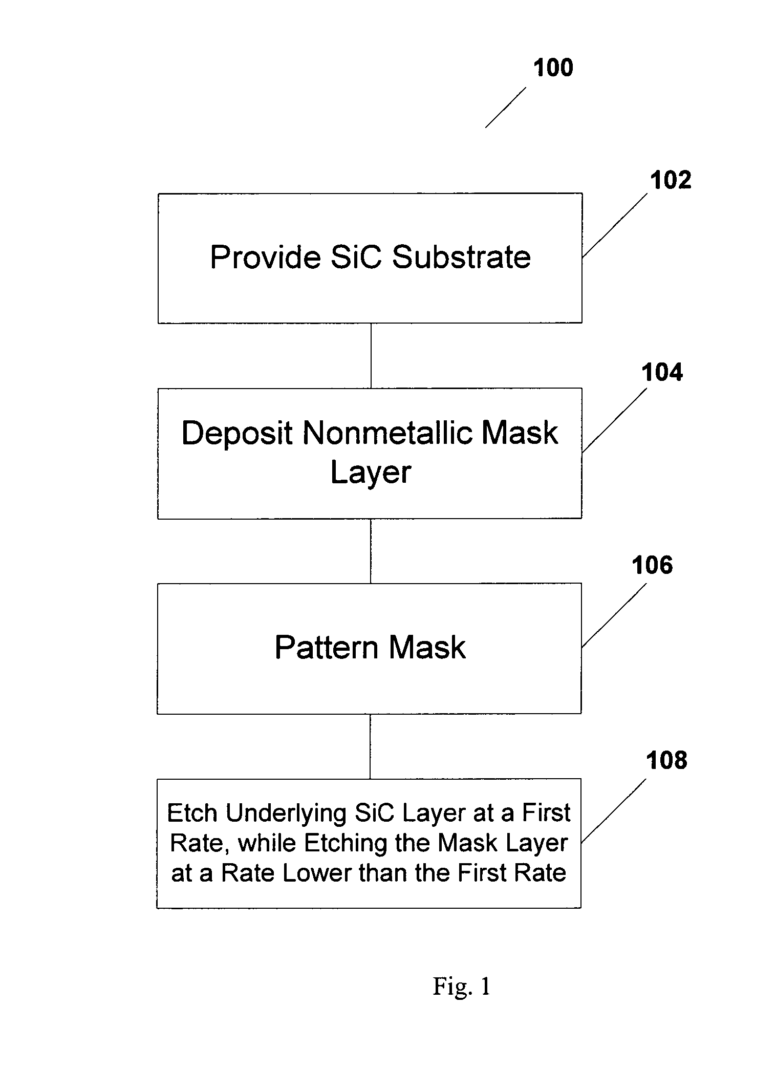
A method of etching silicon carbide using a nonmetallic mask layer. The method includes providing a silicon carbide substrate; forming a non-metallic mask layer by applying a layer of material on the substrate; patterning the mask layer to expose underlying areas of the substrate; and etching the underlying areas of the substrate with a plasma at a first rate, while etching the mask layer at a rate lower than the first rate.

Description

FEDERALLY SPONSORED RESEARCH OR DEVELOPMENT [0001] This invention was made with Government support under Grant (Contract) No. N660010118967 awarded by DARPA, and Grant (Contract) No. 9782 awarded by the Department of Energy / Sandia National Laboratories. The Government has certain rights to this invention.BACKGROUND OF THE INVENTION [0002] The present invention relates to semiconductor processing methods, and in particular to processing techniques for silicon carbide semiconductors. [0003] Silicon carbide (SiC) is well known as an attractive material for electronic devices operating at high temperatures and high power due to its large energy band gap and high breakdown field. SiC also possesses superior mechanical properties and chemical inertness which are of interest in fabricating microelectromechanical systems (MEMS) as well as nanoelectromechanical systems (NEMS) for applications in harsh environments; environments characterized by locations exposed to high temperature, strong r...

Claims


Application Information

Patent Timeline
IPC IPC(8): B81C1/00H01L21/00H01L21/04H01L21/306H01L21/308H01L29/82
CPCB81C1/00595H01L21/0475B81C2201/0132B81C2201/0109
Inventor GAO, DIHOWE, ROGER T.MABOUDIAN, ROYA
Owner RGT UNIV OF CALIFORNIA
Learn More