Method for manufacturing high density non-volatile magnetic memory

a non-volatile magnetic memory and high density technology, applied in the field of manufacturing memory cells, can solve the problem of reducing the program current required to switch the free layer state, and achieve the effect of reducing the program curren

Active Publication Date: 2013-09-19
AVALANCHE TECH
View PDF4 Cites 159 Cited by
  • Summary
  • Abstract
  • Description
  • Claims
  • Application Information

AI Technical Summary

Benefits of technology

[0006]Embodiments of the present invention include methods for manufacturing of a magnetic tunnel junction (MTJ) array on a wafer using double patterning to achieve dense arrays of MTJs exceeding the limit set by the minimum feature size (F) in every technology node. Two orthogonal line patterning steps achieve an array of MTJs located where the orthogonal lines overlap. In addition, a self-aligned double patterning method embodiment allows for a half pitch capability for the packing of the MTJs in the array. T

Problems solved by technology

Reducing the program current required to switch the fre

Method used


Image

  • Method for manufacturing high density non-volatile magnetic memory
  • Method for manufacturing high density non-volatile magnetic memory
  • Method for manufacturing high density non-volatile magnetic memory

Examples


third embodiment

[0032]Alternatively, in the present invention the self-aligned double patterning (SDP) method can be used to form the second set of parallel mask lines which can then be used create the dielectric square or rectangular shape mask pad, similar to the dielectric square or rectangular shape pad 15c as shown in FIG. 6. By using the SDP method for both orthogonal set of mask lines both dimensions can be width F / 2. Similar steps as depicted in FIG. 7 and FIG. 8 can follow to achieve a very dense array of MTJ pillars similar to those shown in FIG. 9.

fourth embodiment

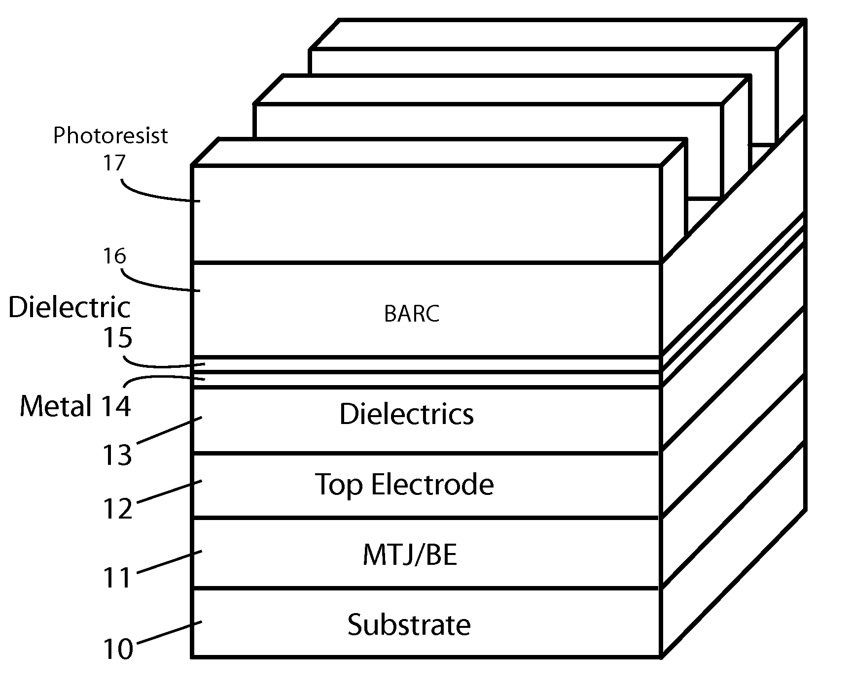
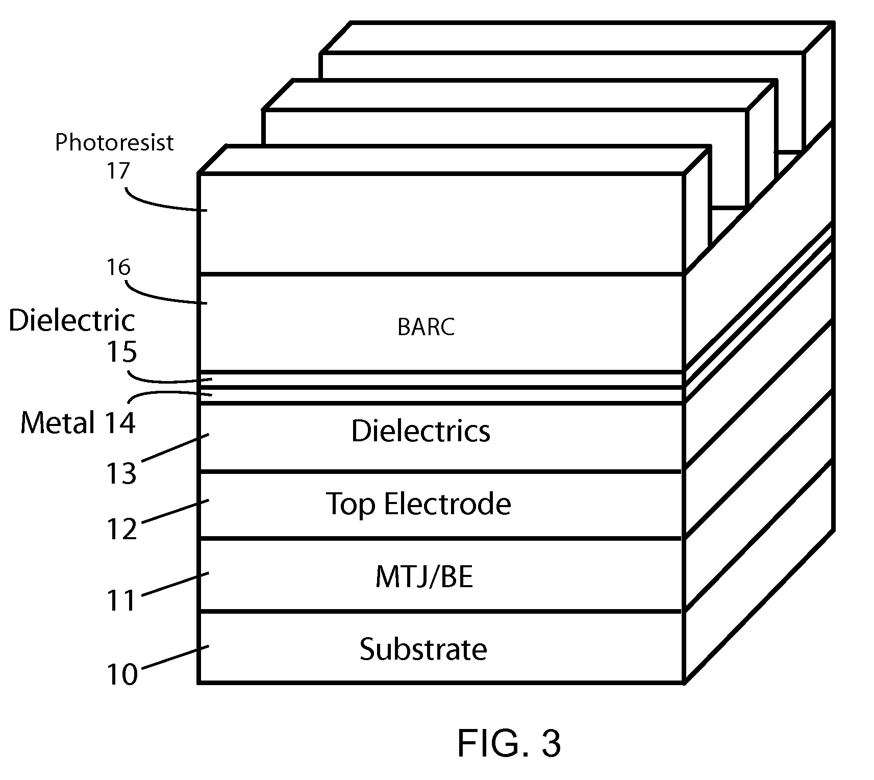
[0033]In the present invention, a modified stack structure and process flow from the previous embodiments is used. The first set of mask lines is used to pattern the MTJ / BE layers into lines before the top electrode layer is deposited. Referring now to FIG. 11, the film stack structure of a non-volatile magnetic memory has been deposited on a substrate 30 containing CMOS circuitry (not shown) and means for electrical connections to the MTJ elements that will be patterned. The stack structure consists of the MTJ layer group which in turn consists of the magnetic layers and tunnel barrier as described above. On top of the MTJ and bottom electrode stack (MTJ / BE) 31, a hard mask layer 32 and then first (lower) dielectric layer 33 is deposited. In a preferred embodiment, the hard mask layer 32 is made out of tantalum (Ta).

[0034]On top of the dielectric layer 33, a thin metal layer and a thin dielectric layer were deposited and then patterned as described above for the first embodiment to...


PUM


Abstract

Methods of fabricating MTJ arrays using two orthogonal line patterning steps are described. Embodiments are described that use a self-aligned double patterning method for one or both orthogonal line patterning steps to achieve dense arrays of MTJs with feature dimensions one half of the minimum photo lithography feature size (F). In one set of embodiments, the materials and thicknesses of the stack of layers that provide the masking function are selected so that after the initial set of mask pads have been patterned, a sequence of etching steps progressively transfers the mask pad shape through the multiple mask layer and down through all of the MTJ cell layers to the form the complete MTJ pillars. In another set of embodiments, the MTJ/BE stack is patterned into parallel lines before the top electrode layer is deposited.

Description

CROSS REFERENCE TO RELATED APPLICATIONS[0001]This application is a continuation-in-part of commonly assigned U.S. patent application Ser. No. 12 / 040,827 filed Feb. 29, 2008.FIELD OF THE INVENTION[0002]The present invention relates generally to non-volatile magnetic random access memory and particularly to methods of manufacturing memory cells for non-volatile magnetic random access memory (MRAM).BACKGROUND[0003]FIGS. 1 and 2 illustrate a selected stage of the prior art fabrication process of a non-volatile MRAM array on a wafer. The stack of thin film layers are deposited on a substrate containing CMOS circuitry (not shown) and landing pads for electrical connections to the bottom electrode (BE) for the magnetic tunnel junction (MTJ) elements. A typical magnetic tunnel junction (MTJ) cell consists of a bottom electrode (BE) and seed layers, followed by an anti-ferromagnetic pinning layer (AFM). The composition of AFM layer is typically alloys of IrMn or PtMn. A fixed magnetic layer ...

Claims


Application Information

Patent Timeline
IPC IPC(8): H01L43/12
CPCB82Y10/00B82Y25/00G11C11/161H01L43/12H01L27/228H10N50/01
Inventor MALMHALL, ROGER KLASSATOH, KIMIHIROZHANG, JINGKESHTBOD, PARVIZRANJAN, RAJIV YADAV
Owner AVALANCHE TECH
Why Eureka
Try Eureka