Forming process of thin film pattern and manufacturing process of device, electro-optical apparatus and electronic apparatus

a technology of electrooptical apparatus and manufacturing process, which is applied in the direction of conductive pattern formation, wheelchair/patient conveyance, instruments, etc., can solve the problems of difficult to cope with a case, and difficulty in obtaining sufficient wiring line width precision, so as to broaden the range of functional liquids

Inactive Publication Date: 2005-01-06
SEIKO EPSON CORP
View PDF11 Cites 31 Cited by
  • Summary
  • Abstract
  • Description
  • Claims
  • Application Information

AI Technical Summary

Benefits of technology

[0009] According to an aspect of invention, because of a construction of arranging the functional liquid for forming the thin film pattern between the banks which are protrudingly set up on the substrate, it is possible to carry out patterning of the thin film pattern smoothly along a shape of the banks to a desired line width. Also, even though part of the ejected functional liquid is deposited on the banks, since the banks are imparted with the liquid repellent property, that part is repelled from the banks and runs down to a bottom part between the banks. Consequently, the functional liquid ejected is properly placed between the banks on the substrate, thereby making it possible to realize a thin line of the thin film pattern formed.
[0010] In this case, the step of processing repellent liquefa...

Problems solved by technology

However, in a case where forming a wiring pattern of a thin line width is attempted based on the process of ejecting liquid droplets, can be difficult to obtain suffici...

Method used


Image

  • Forming process of thin film pattern and manufacturing process of device, electro-optical apparatus and electronic apparatus
  • Forming process of thin film pattern and manufacturing process of device, electro-optical apparatus and electronic apparatus
  • Forming process of thin film pattern and manufacturing process of device, electro-optical apparatus and electronic apparatus

Examples


working example

[0089] Working Example

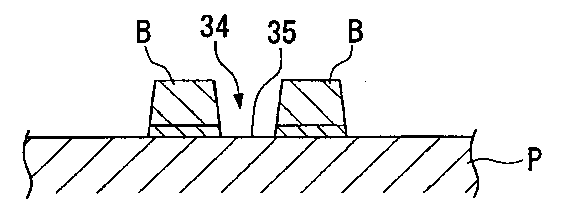
[0090] CF4 plasma processing was carried out to a glass substrate on which are formed banks of an olefin resin using the above-mentioned plasma processing apparatus under processing conditions of a plasma power of 550 W, a carbon tetrafluoride gas flow rate of 100 [mL / min], a He gas flow rate of 10 [L / min], and a moving rate of 2 mm / sec of the above-mentioned sample table 40. A contact angle of an organosilver compound (diethyleneglycol-dimethylether solvent) with respect to the banks after the CF4 plasma processing was measured and it was 66.2 degrees. On the other hand, a contact angle of an organosilver compound (diethyleneglycoldimethylether solvent) with respect to the banks not subjected to the CF4 plasma processing was measured and it was less than 10 degrees. This made it possible to verify that the banks were imparted with the liquid repellent property by the CF4 plasma processing.

[0091] Likewise, the CF4 plasma processing was carried out to a glass su...


PUM


Abstract

The invention provides a forming process of a thin film pattern capable of properly realizing a thin line. The forming process of a thin film pattern of the invention can be a process of forming a thin film pattern by arranging a functional liquid on a substrate P. The process can include a bank forming step to set up banks protrudingly on the substrate corresponding to the thin film pattern, a repellent liquefaction step of imparting a liquid repellent property to the bank by CF4 plasma processing, and a material arranging step of arranging the functional liquid between the banks imparted with the liquid repellent property.

Description

BACKGROUND OF THE INVENTION [0001] 1. Field of Invention [0002] This invention relates to a process of forming a thin film pattern and a manufacturing process of a device, an electro-optical apparatus, and an electronic apparatus. [0003] 2. Description of Related Art [0004] In processing a device having an electronic circuit, an integrated circuit and the like, for example, photolithography can be employed. The photolithography can be made up of coating a photosensitive material called a photoresist on a substrate pretreated with a conductive film, irradiating it with a circuit pattern and developing it, applying photo-etching to the conductive film according to a photoresist pattern, thus producing a thin film wiring pattern. Large-scale equipment and complicated processes, such as vacuum equipment, are required for this photolithography, and further, since efficiency of using materials is of the order of a few percentage points, most of the materials are necessarily discarded. Man...

Claims


Application Information

Patent Timeline
IPC IPC(8): G02F1/13B05D1/26B05D3/04G02F1/1333H01L21/02H01L21/20H01L21/208H01L21/288H01L21/3205H01L21/768H05K3/12
CPCH01L21/288H01L21/3205H01L21/76838H05K3/125H01L21/02422H05K2201/09909H05K2203/1173H01L21/02532H01L21/02639H05K3/1258A61G5/04A61G5/1051Y10S180/907
Inventor HIRAI, TOSHIMITSU
Owner SEIKO EPSON CORP
Why Eureka
Try Eureka