Method of forming silicon carbide films

Active Publication Date: 2005-01-13
ASM JAPAN
View PDF17 Cites 35 Cited by
  • Summary
  • Abstract
  • Description
  • Claims
  • Application Information

AI Technical Summary

Benefits of technology

[0023] A mixture of high and low frequency RF power, such that high frequency RF power is in the range of 13.56 MHz to 30 MHz and low frequency RF power is in the range of 200 kHz to 500 kHz, wherein the ratio of low frequen

Problems solved by technology

Integrated circuits have evolved into complex devices that include multiple levels of metal layers to electrically interconnect discrete layers of semiconductor devices on a single semiconductor chip.
As the device dimensions continuously shrink, the RC time delay of the interconnect system becomes one of the most important limitation factors to the integrated circuits performance.
The use of copper as the interconnect material has various problems.
For example, copper is easily diffused into the low dielectric constant insulating film from the copper wiring, thus increasing the leakage current between the upper and lower wiring.
However, there is no report on the identif

Method used


Image

  • Method of forming silicon carbide films
  • Method of forming silicon carbide films
  • Method of forming silicon carbide films

Examples


Embodiment Construction

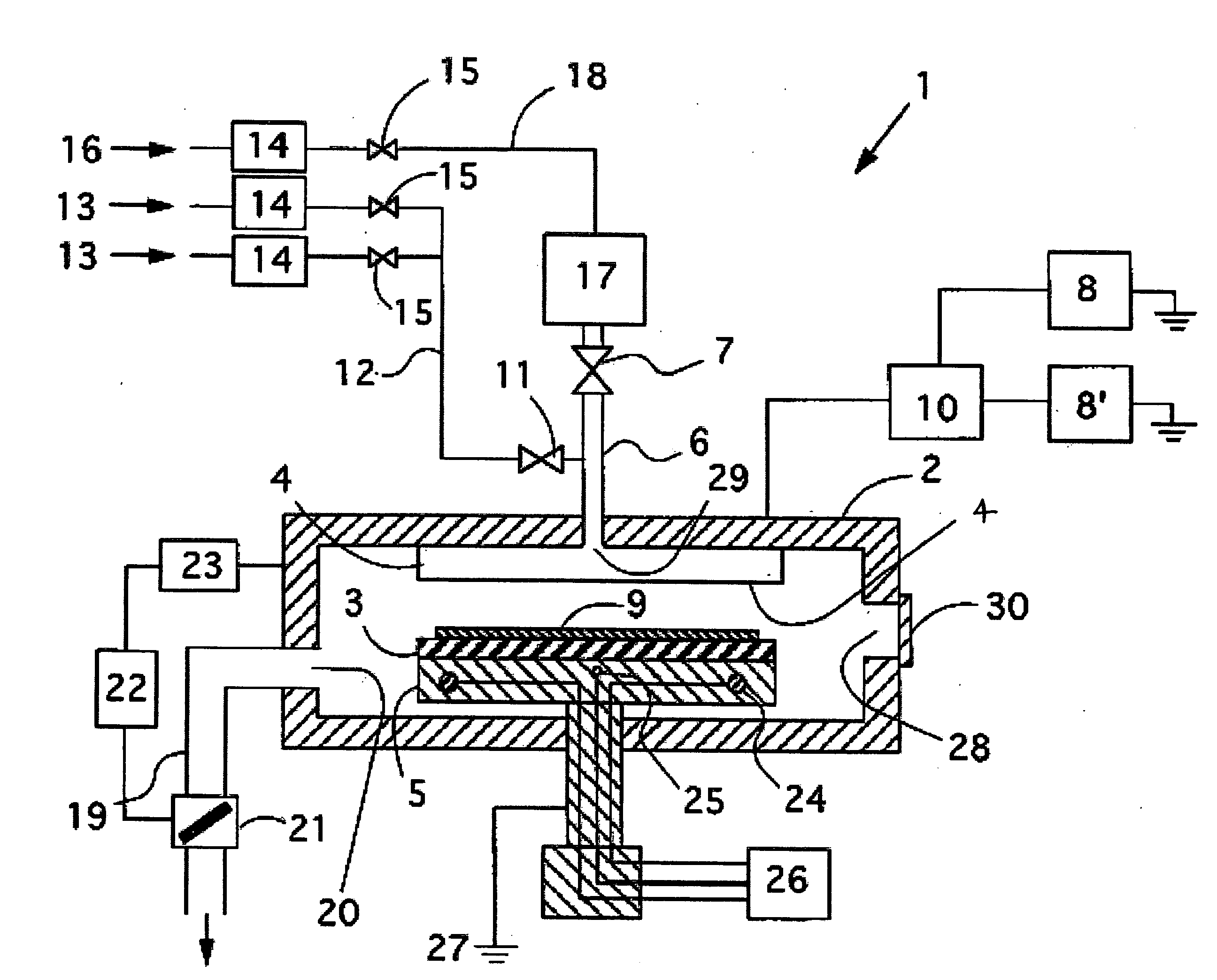
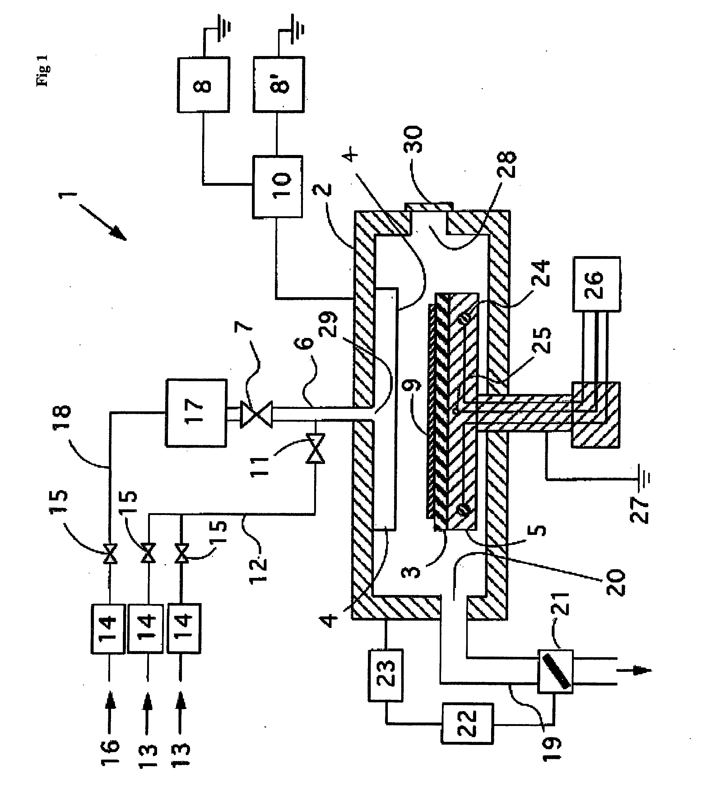
[0027] Disclosed herein is a method for depositing a silicon carbide film having a low dielectric constant with low leakage current and high compressive stress onto a substrate in a CVD chamber, comprising the steps of providing a silicon source, carbon source, nitrogen source and an inert gas in a reaction zone containing a substrate, and reacting the silicon and carbon and nitrogen source in the presence of a plasma to deposit a low dielectric constant and low leakage current silicon carbide film on the substrate.

[0028] A mixture of high and low frequency RF power generates the electric field, wherein the ratio of low frequency to total power is less than about 0.5. The leakage current and dielectric constant in the resulting silicon carbide film is directly related to the carbon concentration, amount of nitrogen and inert gas introduced.

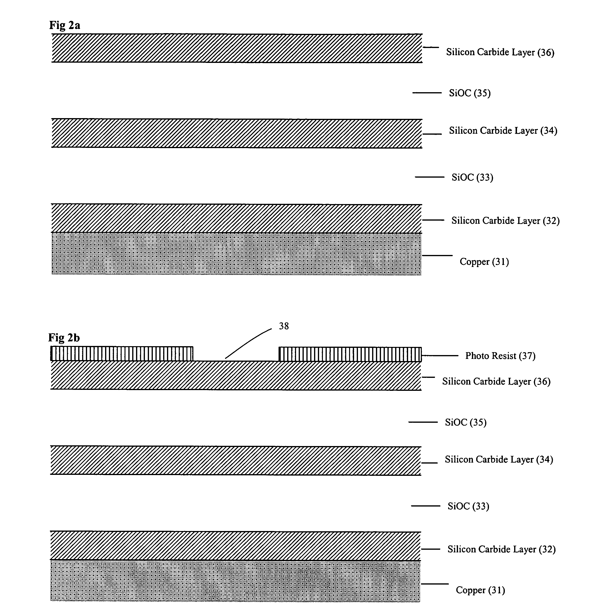
Silicon Carbide Layer Formation

[0029] In one preferred embodiment of the present invention, a silicon carbide layer is formed by reacting a ga...


PUM


Abstract

To deposit silicon onto a substrate, there is introduced into a reaction zone a gas including source gases of silicon, carbon, nitrogen and an inert gas. An electric field is generated using low and high frequency RF power to produce a plasma discharge in the reaction zone to cause the deposition. The average power on the substrate is substantially constant. A ratio of low frequency RF power to total RF power is less than about 0.5.

Description

FIELD OF THE INVENTION [0001] The present invention relates to nitrogen doped silicon carbide layers referred to herein as SiCN and, more particularly to a method of forming low dielectric constant, low leakage current and high compressive stress nitrogen doped silicon carbide layers. BACKGROUND OF THE INVENTION [0002] Integrated circuits have evolved into complex devices that include multiple levels of metal layers to electrically interconnect discrete layers of semiconductor devices on a single semiconductor chip. Recently, with the evolution of higher integration and higher density of integrated circuit components, the demand for greater speed of the data transfer rate is required. For this reason, an insulating film having high compressive stress, low leakage current, low dielectric constant to give the small RC delay is employed. [0003] As the device dimensions continuously shrink, the RC time delay of the interconnect system becomes one of the most important limitation factors...

Claims


Application Information

Patent Timeline
IPC IPC(8): H01L23/522H01L21/285H01L21/314H01L21/768
CPCH01L21/76801H01L21/76829H01L21/76807
Inventor GOUNDAR, KAMAL KISHORE
Owner ASM JAPAN
Why Eureka
Try Eureka