Alloy type semiconductor nanocrystals and method for preparing the same

a technology of alloy-type semiconductors and nanocrystals, which is applied in the direction of crystal growth process, nanoinformatics, transportation and packaging, etc., can solve the problems of difficult to form reproducible and uniform quantum structures in solvents containing large amounts of impurities, and the method has a restriction on the solvent used, so as to achieve uniform sizes and shapes, high quantum efficiency

Active Publication Date: 2005-01-20
SAMSUNG ELECTRONICS CO LTD
View PDF8 Cites 133 Cited by
  • Summary
  • Abstract
  • Description
  • Claims
  • Application Information

AI Technical Summary

Benefits of technology

[0011] The present invention provides alloy type Group 12-16 compound semiconductor nanocrystals which are stable and have a high quantum efficiency and uniform sizes and shapes.

Problems solved by technology

Even though quantum dots grown mainly by lattice mismatch using a vapor phase method have good crystallinity, the vapor phase method has a fatal defect in controlling the size, uniformity, and density of the quantum dots, which renders fabrication of commercially available semiconductor devices difficult.
However, this method has a restriction on the solvent used, i.e., tri-octyl phophonic acid (referred to as TOPO, hereinafter).
Reportedly, it is difficult to form reproducible and uniform quantum structures in a solvent containing a large amount of impurities.
It is also reported that impurities in the technical grade TOPO serves as an uncontrollable reaction parameter that adversely affects the reaction.
In this case, however, a change in a binding property of TOPO may occur, which renders the growth of desired crystals difficult.

Method used


Image

  • Alloy type semiconductor nanocrystals and method for preparing the same
  • Alloy type semiconductor nanocrystals and method for preparing the same
  • Alloy type semiconductor nanocrystals and method for preparing the same

Examples


example 1

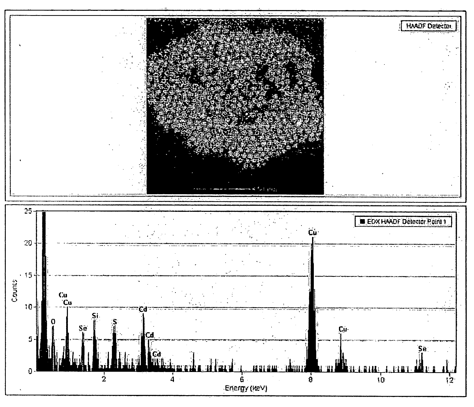
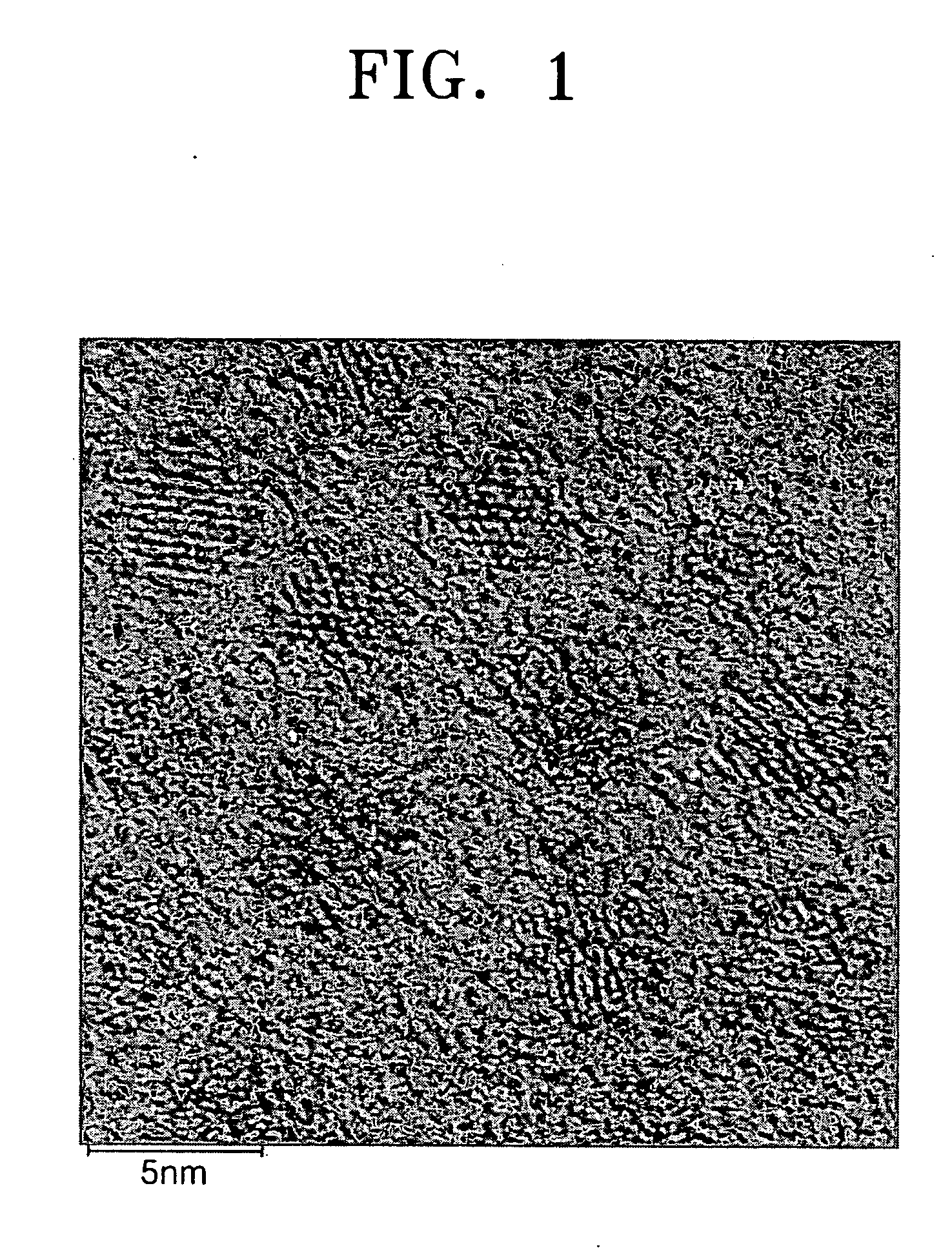
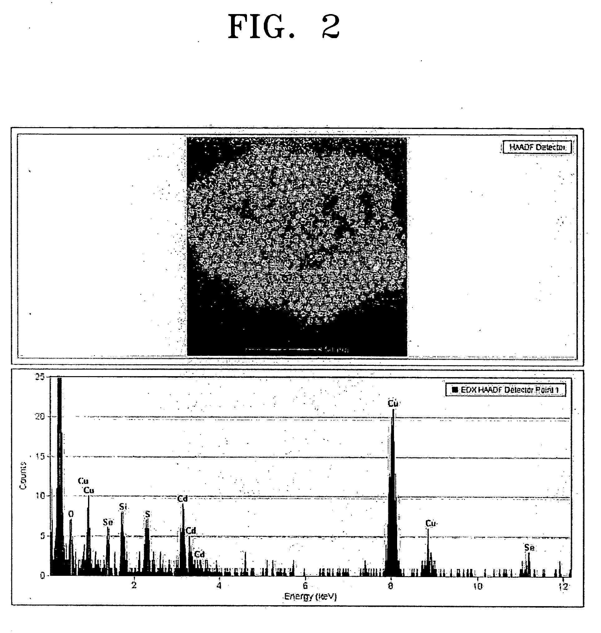
Preparation of CdSeS Nanocrystals

[0063] 16 g of tri-octyl amine (referred to as TOA, hereinafter), 0.5 g of oleic acid, and 0.4 mmol of CdO were simultaneously placed in a 100 ml flask provided with a reflux condenser and stirred at 300° C. to obtain a Cd precursor solution.

[0064] Separately, Se powders were dissolved in tri-octyl phosphine (referred to as TOP, hereinafter) to obtain a Se-TOP complex solution with a Se concentration of about 0.1M. S powders were dissolved on TOP to obtain S-TOP complex solution with a S concentration of about 4M.

[0065] 0.5 ml of S-TOP complex solution 0.5 ml of the Se-TOP complex solution were rapidly added to the Cd precursor solution and stirred for about 4 minutes.

[0066] When the reaction of the resultant mixture was terminated, the reaction temperature was rapidly reduced to room temperature and then centrifugation was performed with addition of an ethanol as a non-solvent. A supernatant was decanted and discarded. A precipitate was disperse...

example 2

Preparation of ZnCdSe Nanocrystals

[0072] 16 g of TOA, 0.5 g of oleic acid, 0.2 mmol of zinc acetyl acetonate, and 0.2 mmol of cadmium (Cd) oxide were simultaneously placed in a 100 ml flask provided with a reflux condenser and stirred at 300° C. to obtain a Zn and Cd precursor solution.

[0073] Separately, Se powders were dissolved in TOP to obtain a Se-TOP complex solution with a Se concentration of about 0.25M. 1 ml of the Se-TOP complex solution was rapidly added to the Zn and Cd precursor solution and stirred for about 2 minutes.

[0074] When the reaction of the resultant mixture was terminated, the reaction temperature was rapidly reduced to room temperature and then centrifugation was performed with addition of an ethanol as a non-solvent. A supernatant was decanted and discarded. A precipitate was dispersed in a toluene and then a PL spectrum in the solution was measured.

[0075] The PL spectrum showed an emission wavelength of about 456 nm and FWHM of about 26 nm.

example 3

Preparation of CdSe / CdS Nanocrystals

[0076] 16 g of TOA, 0.5 g of oleic acid, and 0.4 mmol of cadmium acetate were simultaneously placed in a 100 ml flask provided with a reflux condenser and stirred at 300° C. to obtain a Cd precursor solution.

[0077] Separately, Se powders were dissolved in TOP to obtain a Se-TOP complex solution with a Se concentration of about 0.25M. 1 ml of the Se-TOP complex solution was rapidly added to the Cd precursor solution and stirred for about 4 minutes.

[0078] S powders were dissolved in TOP to obtain a S-TOP complex solution with a S concentration of about 2 M. 1 ml of the S-TOP complex solution was dropwise added to the CdSe-containing solution and stirred.

[0079] When the reaction of the resultant mixture was terminated, the reaction temperature was rapidly reduced to room temperature and then centrifugation was performed with addition of an ethanol as a non solvent. A supernatant was decanted and discarded. A precipitate was dispersed in a toluene...


PUM

PropertyMeasurementUnit
temperatureaaaaaaaaaa
FWHMaaaaaaaaaa

Abstract

Provided is a chemical wet preparation method for Group 12-16 compound semiconductor nanocrystals. The method includes mixing one or more Group 12 metals or Group 12 precursors with a dispersing agent and a solvent followed by heating to obtain a Group 12 metal precursor solution; dissolving one or more Group 16 elements or Group 16 precursors in a coordinating solvent to obtain a Group 16 element precursor solution; and mixing the Group 12 metal precursors solution and the Group 16 element precursors solution to form a mixture, and then reacting the mixture to grow the semiconductor nanocrystals. The Group 12-16 compound semiconductor nanocrystals are stable and have high quantum efficiency and uniform sizes and shapes.

Description

BACKGROUND OF THE INVENTION [0001] This application claims priority from Korean Patent Application No. 2003-49547, filed on Jul. 19, 2003, in the Korean Intellectual Property Office, the disclosure of which is incorporated herein in its entirety by reference. [0002] 1. Field of the Invention [0003] The present invention relates to alloy type semiconductor nanocrystals and a method of preparing the same. More particularly, the present invention relates to alloy type Group 12-16 compound semiconductor nanocrystals with a high luminance efficiency in a visible light band and a wet preparation method for the semiconductor nanocrystals. [0004] 2. Description of the Related Art [0005] When compound semiconductor materials are made into nanometer-sized crystals, a quantum confinement effect occurs at the regions of the crystals smaller than the bulk exciton Bohr radius. Such a quantum confinement effect results in a change in bandgap energy which is intrinsic characteristics of semiconduct...

Claims


Application Information

Patent Timeline
Patent Type & Authority Applications(United States)
IPC IPC(8): B82Y20/00H05B33/14C01B17/20C01B19/00C09K11/00C09K11/08C09K11/56C09K11/88C09K11/89H01L21/20H01L21/208H01L21/368H01L29/06H01L31/0256H01L51/00H01L51/42H01L51/50H05B33/00
CPCB82Y10/00Y10T428/2982B82Y30/00C01B17/20C01B19/007C01P2002/72C01P2002/84C01P2002/85C01P2004/04C01P2004/52C09K11/883H01L29/0665H01L29/0673H01L51/0059H01L51/0081H01L51/4213H01L51/5012H05B33/14C30B7/00C30B7/005H01L21/02551H01L21/02557H01L21/0256H01L21/02601H01L21/02628Y10S977/777Y10S977/824Y10S977/825Y10S977/784Y10S977/785Y10T428/2991Y10T428/12028Y10T428/12049Y10T428/12181B82Y20/00H10K85/631H10K85/324H10K30/10H10K50/11
Inventor JANG, EUN-JOOAHN, TAE-KYUNG
Owner SAMSUNG ELECTRONICS CO LTD
Why Eureka
Try Eureka