EL display device and a method of manufacturing the same

Inactive Publication Date: 2005-01-20
SEMICON ENERGY LAB CO LTD
View PDF98 Cites 117 Cited by
  • Summary
  • Abstract
  • Description
  • Claims
  • Application Information

AI Technical Summary

Benefits of technology

[0028] Accordingly, with the employment of the thin film deposition apparatus, the three types of light emitting layers luminescing red, green, and blue can be formed at the same time. Consequently, light-emitting layers made of a high molecular organic EL materia

Problems solved by technology

In particular, the active matrix EL display device is currently attracting much attention.
Hence, if the distance between the application surface and the nozzle of the ink-jet head

Method used


Image

  • EL display device and a method of manufacturing the same
  • EL display device and a method of manufacturing the same
  • EL display device and a method of manufacturing the same

Examples


Example

Embodiment 1

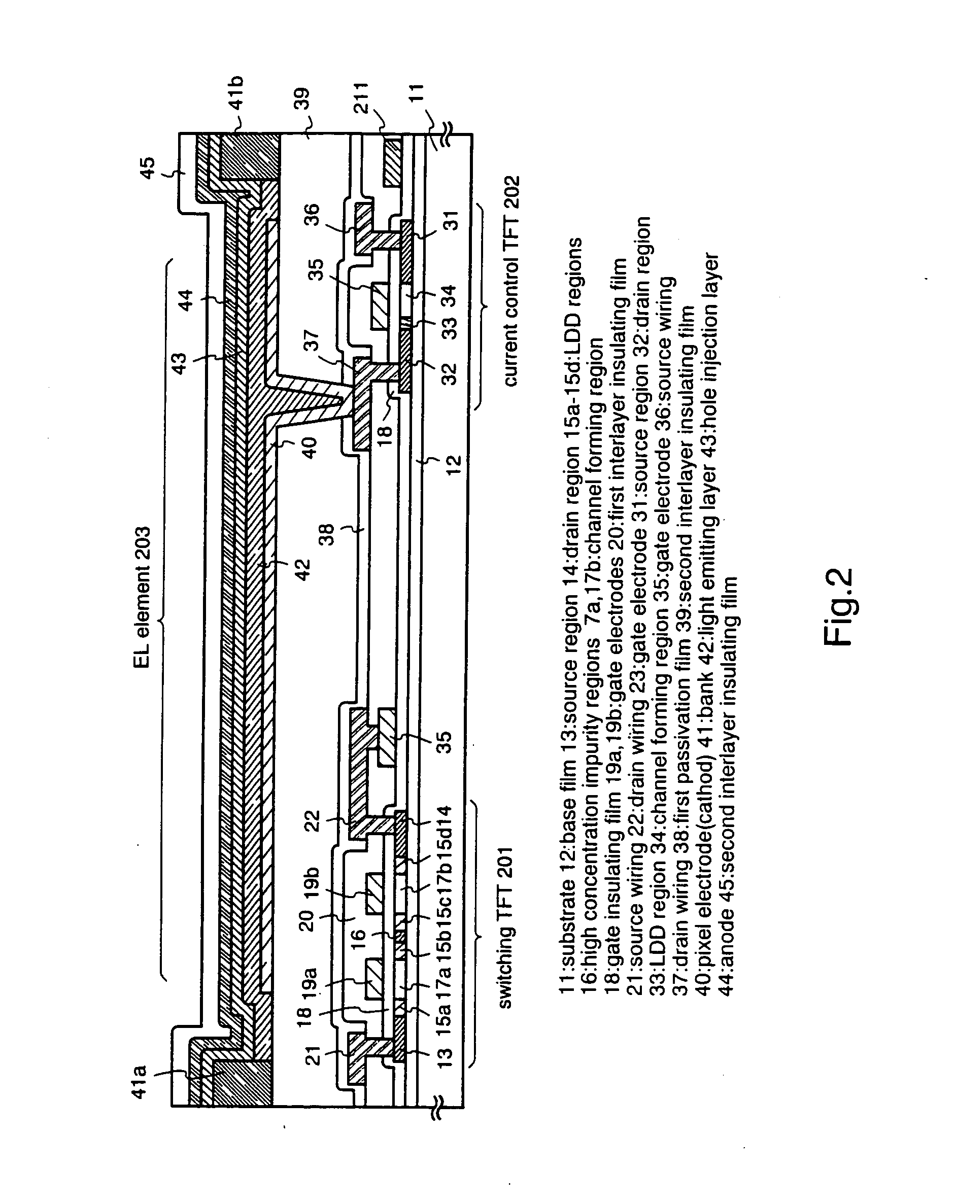
[0110] The embodiments of the present invention are explained using FIGS. 4A to 6C. A method of simultaneous manufacture of a pixel portion, and TFTs of a driver circuit portion formed in the periphery of the pixel portion, is explained here. Note that in order to simplify the explanation, a CMOS circuit is shown as a basic circuit for the driver circuits.

[0111] First, as shown in FIG. 4A, a base film 301 is formed to a thickness of 300 nm on a glass substrate 300. Silicon oxide nitride films are laminated as the base film 301 in Embodiment 1. At this point, it is appropriate to set the nitrogen concentration to between 10 and 25 wt % in the film contacting the glass substrate 300. In addition, it is effective that the base film 301 has a thermal radiation effect, and a DLC (diamond-like carbon) film may also be provided.

[0112] Next, an amorphous silicon film (not shown in the figures) is formed with a thickness of 50 nm on the base film 301 by a known deposition meth...

Example

Embodiment 2

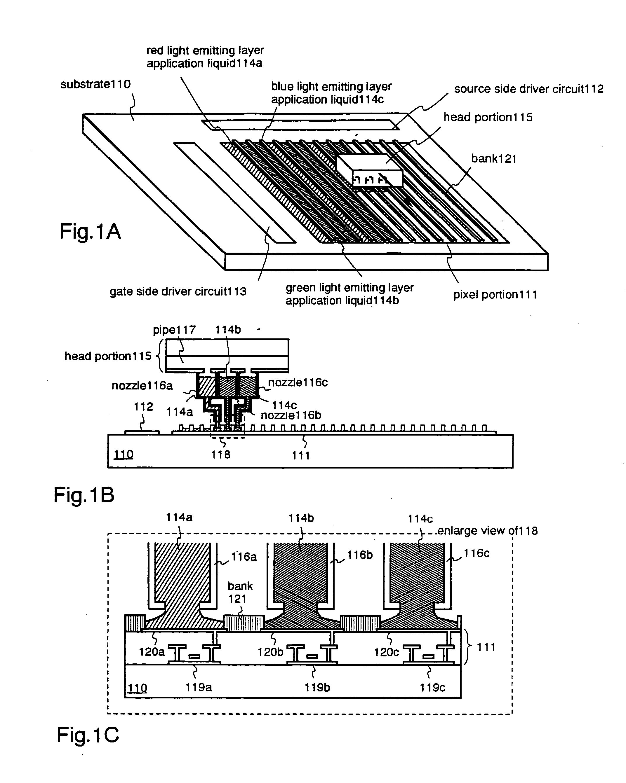
[0183] An example of simultaneously forming, in a lengthwise direction or a lateral direction, three types of stripe shape light emitting layers luminescing red, green, and blue color lights was shown in Embodiment 1. An example of a stripe shape light emitting layer formed by dividing it into a plural number of divisions in a longitudinal direction is shown in Embodiment 2.

[0184] As shown in FIG. 12A, the pixel portion 111, the source side driver circuit 112, and the gate side driver circuit 113, all formed of TFTs, are formed on the substrate 110. The pixel portion 111 is partitioned into matrix by a bank 1201. In the case of Embodiment 2, a plurality of pixels 1203 are arranged within one of the squares 1202 partitioned by the bank 1201 as shown in FIG. 12B. However, the number of pixels is not limited.

[0185] In such a state, the film deposition process of an organic EL material for functioning as a light emitting layer is carried out using the thin film deposition...

Example

Embodiment 3

[0191] A case of employing the present invention in a passive type (simple matrix type) EL display device is explained in Embodiment 3 with reference to FIG. 13. In FIG. 13, reference numeral 1301 denotes a plastic substrate and 1302 denotes a cathode made of an aluminum alloy film. The cathode 1302 is formed by the evaporation method in Embodiment 3. Note that although not shown in FIG. 13, a plural number of lines of cathodes are arranged in a stripe shape, in a perpendicular direction on a defined space.

[0192] Further, a bank 1303 is formed so as to fill up the spaces between the cathodes 1302 arranged in stripes. The bank 1303 is formed along the cathodes 1302 in a perpendicular direction on the defined space.

[0193] Subsequently, light emitting layers 1304a to 1304c made of a high molecular organic EL material are formed by the film deposition method employing the thin film deposition apparatus of FIG. 1. Of course, reference numeral 1304a is a light emitting laye...


PUM


Abstract

To provide a high throughput film deposition means for film depositing an organic EL material made of polymer accurately and without any positional shift. A pixel portion is divided into a plurality of pixel rows by a bank, and a head portion of a thin film deposition apparatus is scanned along a pixel row to thereby simultaneously apply a red light emitting layer application liquid, a green light emitting layer application liquid, and a blue light emitting layer application liquid in stripe shapes. Heat treatment is then performed to thereby form light emitting layers luminescing each of the colors red, green, and blue.

Description

BACKGROUND OF THE INVENTION [0001] 1. Field of the Invention [0002] The present invention relates to an EL display device comprising an EL element, which is constructed of a light emitting organic material capable of obtaining EL (Electro Luminescence)(hereinafter referred to as organic EL material) sandwiched between an anode and a cathode, that is formed on a substrate, and to a method of manufacturing an electronic device (electronic equipment) having the El display device as a display portion (a display or a display monitor). It is to be noted that the above-mentioned EL display device is also referred to as OLED (Organic Light Emitting Diodes). [0003] 2. Description of the Related Art [0004] In recent years, the development of a display device (EL display device) employing an EL element as a self-emissive element that utilizes the EL phenomenon of a light emitting organic material is proceeding. Since the EL display device is a self-emissive type, it does not need a backlight s...

Claims


Application Information

Patent Timeline
IPC IPC(8): H01L27/32H01L51/00H01L31/12H01L51/40H01L51/52H05B33/02H05B33/04H05B33/10
CPCH01L27/322H01L27/3244H01L2251/5315H01L51/0005H01L51/5237H01L51/0003H10K59/38H10K59/124H10K71/135H10K50/846H10K50/8426H10K2102/3026H10K71/851H01L31/12H05B33/02H05B33/10H10K71/12H10K50/84H10K59/12
Inventor YAMAZAKI, SHUNPEIYAMAMOTO, KUNITAKAHIROKI, MASAAKIFUKUNAGA, TAKESHI
Owner SEMICON ENERGY LAB CO LTD
Why Eureka
Try Eureka