

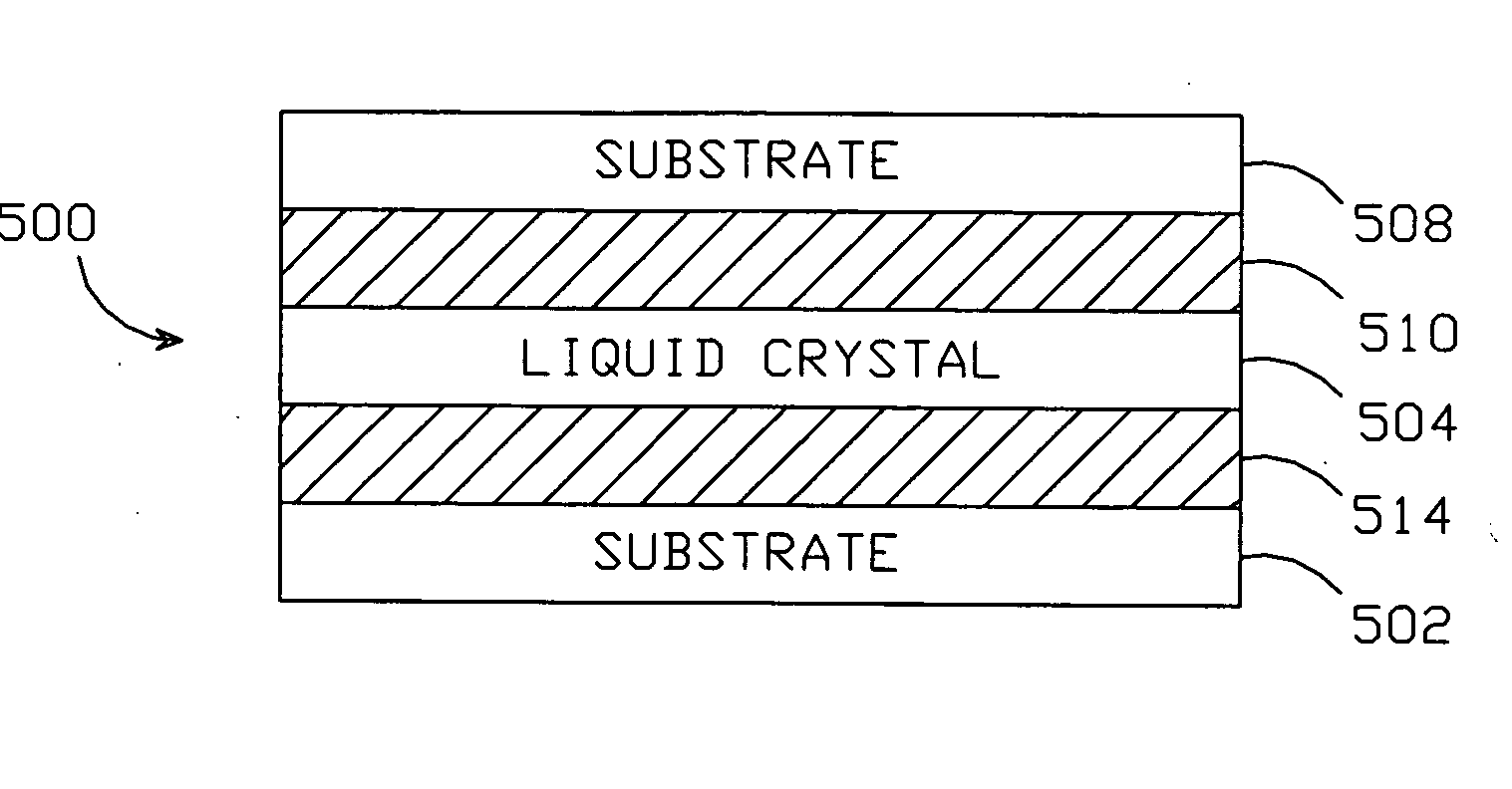
Thin film infrared transparent conductor
a transparent conductor and thin film technology, applied in the field of transparent conductive thin films, can solve the problems of limited utility of other possible optically transparent conductive materials such as doped semiconductor wafers or epitaxial layers (si, ge, gaas, etc., and achieve the effect of suitable electrical conductivity and high optical transmission
- Summary
- Abstract
- Description
- Claims
- Application Information
AI Technical Summary
Benefits of technology
Problems solved by technology
Method used
Image

Examples
example 1
Growth of Indium Doped CdO (“CdO:In”) by PLD
A ceramic target comprising In2O3 and CdO was placed in the target holder of the PLD chamber about 10 inches away from an MgO substrate. The target was prepared by mixing 1% by weight In2O3 powder with 99% by weight CdO powder in a jar, filling the jar with a quantity of methanol approximately equal in volume to the CdO / In2O3 mixture to form a slurry, and adding a like volume of ceramic beads (approximately 1 cm in diameter) to the mixture. The mixture was then “rolled” for 24 hours, the process being known as “ball milling”. The methanol was then evaporated from the mixture and the beads were sifted out. The remaining powder was pressed into a cylindrical shape and sintered in a high temperature furnace (about 1100° C.) to form a ceramic target.
The target was then placed in a vacuum chamber having an O2 partial pressure of approximately 5-50 millitorr and the temperature of the substrate was raised to 440° C. The target was irradiated...
PUM
| Property | Measurement | Unit |
|---|---|---|
| Temperature | aaaaa | aaaaa |
| Length | aaaaa | aaaaa |
| Length | aaaaa | aaaaa |
Abstract
Description
Claims
Application Information