Electron emission device

a technology of electron emission and electronic devices, which is applied in the direction of instruments, tubes with screens, tubes with electrostatic controls, etc., can solve the problems of low current capability, poor input circuit characteristics of such devices, and place a limit on both the miniaturization and switching speed of such devices, so as to facilitate the manufacture and operation of electronic devices. , to achieve the effect of improving the performance of electronic devices

Active Publication Date: 2005-01-27
YEDA RES & DEV CO LTD
View PDF67 Cites 18 Cited by
  • Summary
  • Abstract
  • Description
  • Claims
  • Application Information

AI Technical Summary

Benefits of technology

[0009] There is a need in the art to significantly improve the performance of electronic devices in general and transistors in particular and facilitate their manufacture and operation, by providing a novel electron emission device.

Problems solved by technology

A fundamental drawback of active electronic devices based on semiconductors is that electrons transport is impeded by the semiconductor crystal lattice, which places a limit on both the miniaturization and the switching speed of such devices.
However, their input circuit (control loop) characteristics are relatively poor: they have low current capabilities, low transconductance, high modulation / turn-on voltage and poor noise characteristics.
As a result, despite the: tremendous research efforts in this field, these devices found only very few applications, especially as RF signal amplifiers and sources [S. Iannazzo, Solid State Electronics, 36, 3, 301 (1993)].
Because of the intrinsic resistivity of these devices, the electrons' transmission through the device causes the creation of heat.
This heat is the main obstacle in the attempts to maximize the number of transistors within an integrated circuit per a given area.
However, they suffer from disadvantages in that they are unstable, have relatively short lifetime, and require relatively high voltages for their operation.

Method used


Image

  • Electron emission device
  • Electron emission device
  • Electron emission device

Examples


Embodiment Construction

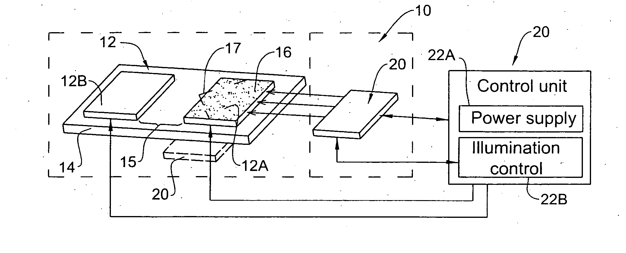
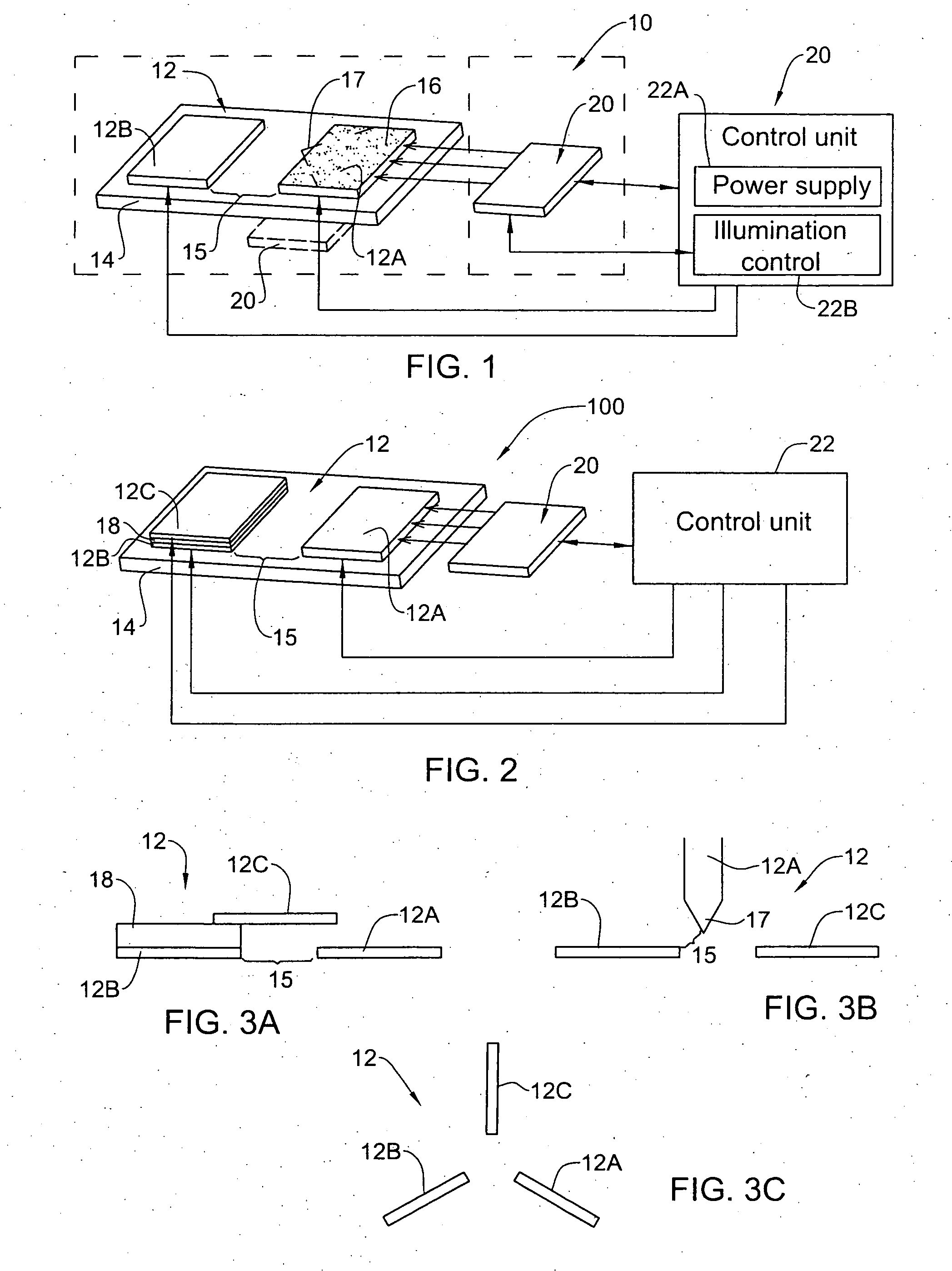
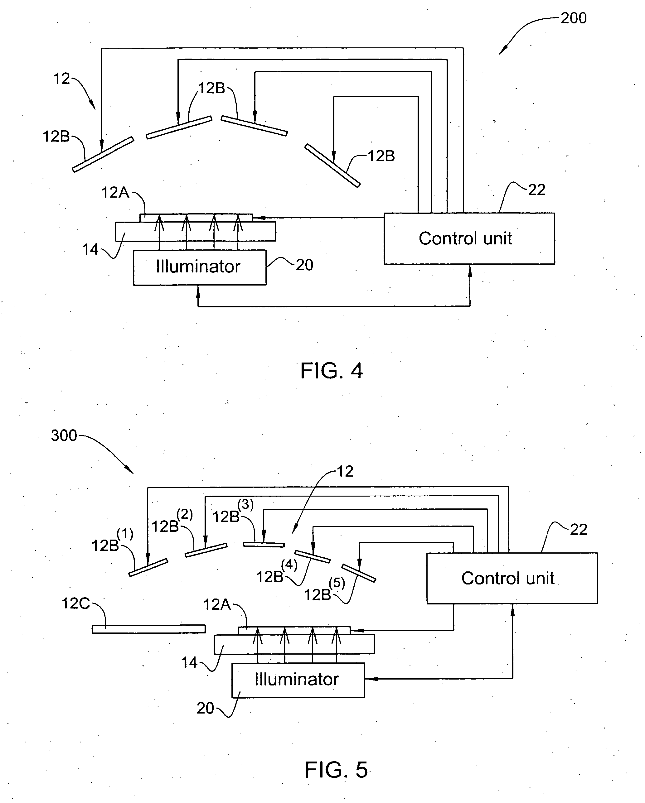
[0050] Referring to FIG. 1, there is schematically illustrated an electronic device 10 constructed according to one embodiment of the invention. The device is configured and operable as an electron photoemission switching device. In the present example, the device has a diode structure configuration. The device 10 comprises an electrodes' arrangement 12 formed by a first Cathode electrode 12A and a second Anode electrode 12B that are arranged on top of a substrate 14 in a spaced-apart relationship with a gap 15 between them. The device is configured to expose the Cathode 12A to exciting radiation to cause electrons emission therefrom towards the Anode. As shown in the present example, the device includes an illuminator assembly 20 oriented and operable to illuminate at least the Cathode electrode 12A to thereby cause emission of electrons from the Cathode towards the Anode.

[0051] The switching (i.e., affecting of an electric current between the Cathode and Anode) is controlled by t...


PUM

PropertyMeasurementUnit
lengthaaaaaaaaaa
electric fieldaaaaaaaaaa
work functionaaaaaaaaaa

Abstract

An electrons' emission device is presented. The device comprises an electrodes' arrangement including at least one Cathode electrode and at least one Anode electrode, the Cathode and Anode electrodes being arranged in a spaced-apart relationship; the device being configured to expose said at least one Cathode electrode to exciting illumination to thereby cause electrons' emission from said Cathode electrode, the device being operable as a photoemission switching device.

Description

FIELD OF THE INVENTION [0001] This invention relates to an electron emission device, such as a diode or triode structure. BACKGROUND OF THE INVENTION [0002] Diode and triode devices are widely used in the electronics. One class of these devices utilize the principles of vacuum microelectronics, namely, their operation is based on ballistic movement of electrons in vacuum [Brodie, Keynote address to the first international vacuum microelectronics conference, June 1988, IEEE Trans. Electron Devices, 36, 11 pt. 2 2637, 2641 (1989); I. Brodie, C. A. Spindt, in “Advances in Electronics and Electron Physics”, vol. 83 (1992), p. 1-106]. According to the principles of vacuum microelectronics, electrons are ejected from a cathode electrode by field emission and tunnel through the barrier potential, when a very high electric field (more than 1 V / nm) is locally applied [R. H. Fowler, L. W Nordheim, Proc. Royal Soc. London A119(1928), p. 173]. [0003] U.S. Pat. No. 5,834,790 discloses a vacuum m...

Claims


Application Information

Patent Timeline
Patent Type & Authority Applications(United States)
IPC IPC(8): C25C3/00G09G3/10H01J1/00H01J1/304H01J1/34H01J3/02H01J21/10H01J31/12H01J40/06
CPCH01J21/10H01J3/021G09G3/22H01J1/30H01J1/34
Inventor NAAMAN, RONHALAHMI, EREZ
Owner YEDA RES & DEV CO LTD
Why Eureka
Try Eureka