Selective etch process of a sacrificial light absorbing material (SLAM) over a dielectric material

a light absorbing material and selective etching technology, applied in the direction of decorative surface effects, electrical appliances, decorative arts, etc., can solve the problems of complex integrated circuits, many challenges in the patterning process, and the application of this technique to dual damascene patterning for sub-0.18 micron technology, and achieves serious challenges in post-etch feature profile control and defect elimination

Inactive Publication Date: 2005-02-10
APPLIED MATERIALS INC
View PDF16 Cites 44 Cited by
  • Summary
  • Abstract
  • Description
  • Claims
  • Application Information

AI Technical Summary

Problems solved by technology

Integrated circuits have evolved into complex devices that can include millions of components (e.g., transistors, capacitors and resistors) on a single chip.
The adoption of dual damascene copper metallization posed many challenges to the patterning process.
However, applying this technique to dual damascene patterning for sub-0.18 micron technology faces serious challenges in defect elimination and post-etch feature profile control.
However, the process requires a wet clean step to remove the remaining SLAM and etch residue.
A wet clean step in a separate process system is time consuming and is limiting in its capability to control the post-etch feature profile.

Method used


Image

  • Selective etch process of a sacrificial light absorbing material (SLAM) over a dielectric material
  • Selective etch process of a sacrificial light absorbing material (SLAM) over a dielectric material
  • Selective etch process of a sacrificial light absorbing material (SLAM) over a dielectric material

Examples


Embodiment Construction

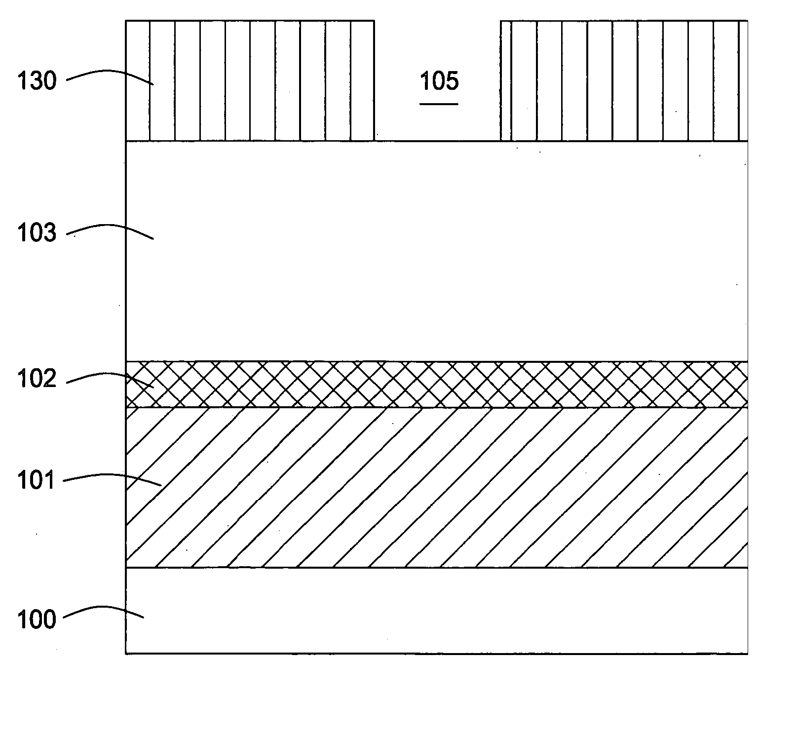
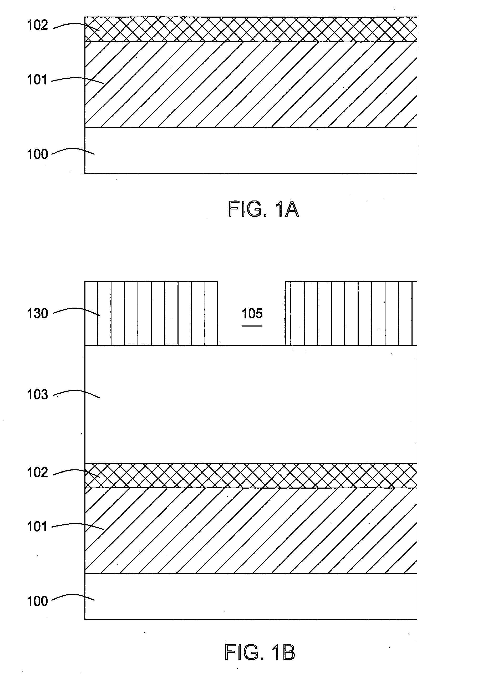
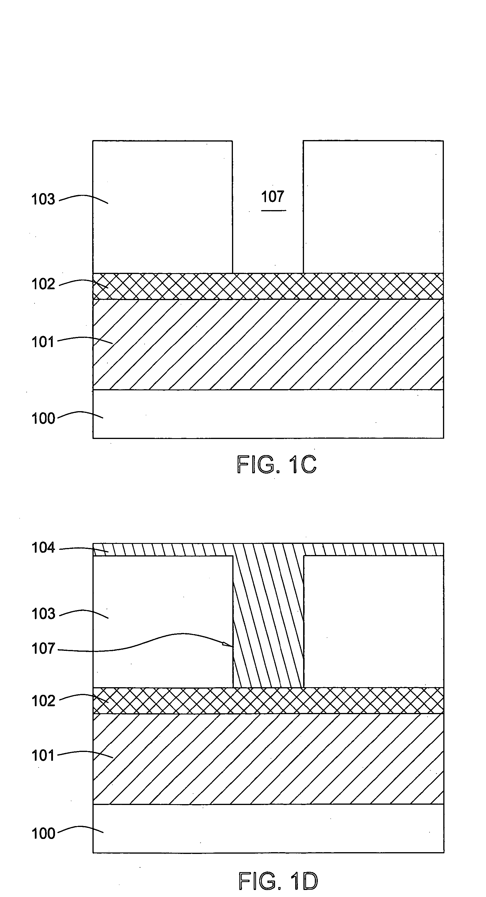
The invention is described within the context of a method of forming a dual damascene structure. Although use of the invention to form a dual damascene structure is one embodiment of the invention, those skilled in the art will understand that the invention may find use in any embodiment where sacrificial light absorbing material (SLAM) residue is etched. FIGS. 1A-1I illustrate cross-sectional views that show structures that result after various processing steps to make a copper containing dual damascene interconnect structure. For clarity, these figures are not drawn to scale. A first conductive layer 101 is formed on substrate 100. The conductive layer 101 may be made from materials conventionally used to form conductive layers for integrated circuits, such as copper, copper alloy, aluminum, aluminum alloy, polysilicon, silicide and the like. After forming the conductive layer 101 on substrate 100, a barrier layer 102 is formed on the conductive layer 101.

Barrier layer 102 will...


PUM

PropertyMeasurementUnit
bias poweraaaaaaaaaa
source poweraaaaaaaaaa
temperatureaaaaaaaaaa

Abstract

A process of selectively etching a sacrificial light absorbing material (SLAM) over a dielectric material, such as carbon doped oxide, on a substrate using a plasma of a gas mixture in a plasma etch chamber. The gas mixture comprises a hydrofluorocarbon gas, an optional hydrogen-containing gas, an optional fluorine-rich fluorocargon gas, a nitrogen gas, an oxygen gas, and an inert gas. The process could provide a SLAM to a dielectric material etching selectivity ratio greater than 10:1.

Description

BACKGROUND OF THE INVENTION 1. Field of the Invention The present invention generally relates to a method of removing a sacrificial light absorbing material and polymer residues that may remain on a substrate surface and inside openings during damascene structure preparation. 2. Description of the Related Art Integrated circuits have evolved into complex devices that can include millions of components (e.g., transistors, capacitors and resistors) on a single chip. The evolution of chip designs continually requires faster circuitry and greater circuit density. The demands for greater circuit density necessitate a reduction in the dimensions of the integrated circuit components. A dual damascene process is used to create the multi-level, high density metal interconnections needed for advanced, high performance integrated circuits (ICs). The initial transition to dual damascene employed copper metal with traditional silicon dioxide dielectric. More recently, the trend has moved to...

Claims


Application Information

Patent Timeline
Patent Type & Authority Applications(United States)
IPC IPC(8): B44C1/22C03C15/00C03C25/68C23F1/00H01L21/311H01L21/768
CPCH01L21/76808H01L21/31116
Inventor CHAE, HEE YEOPPENDER, JEREMIAH T.P.DELGADINO, GERARDO A.ZHAO, XIAOYEYE, YAN
Owner APPLIED MATERIALS INC
Why Eureka
Try Eureka