Projection exposure method and projection exposure system

Inactive Publication Date: 2005-02-10
CARL ZEISS SMT GMBH
View PDF17 Cites 714 Cited by
  • Summary
  • Abstract
  • Description
  • Claims
  • Application Information

AI Technical Summary

Benefits of technology

[0029] In order to avoid defocusing errors, the part of the substrate to be exposed should bear as effectively as possible against the substrate-side plane surface. If this cannot be achieved simply by laying the plane plate on, it is also possible for the substrate to be actively pressed against the substrate-side plane surface so as to produce physical contact, at least during the exposure. It is possible for this purpose, for example, to produce an overpressure, which presses the substrate

Problems solved by technology

The shortening of the operating wavelength λ in the region below 193 nm is rendered difficult by virtue of the fact that only a few sufficiently transparent materials, in particular fluoride crystals such as calcium fluoride or barium fluoride, are available for manufacturing

Method used


Image

  • Projection exposure method and projection exposure system
  • Projection exposure method and projection exposure system
  • Projection exposure method and projection exposure system

Examples


Embodiment Construction

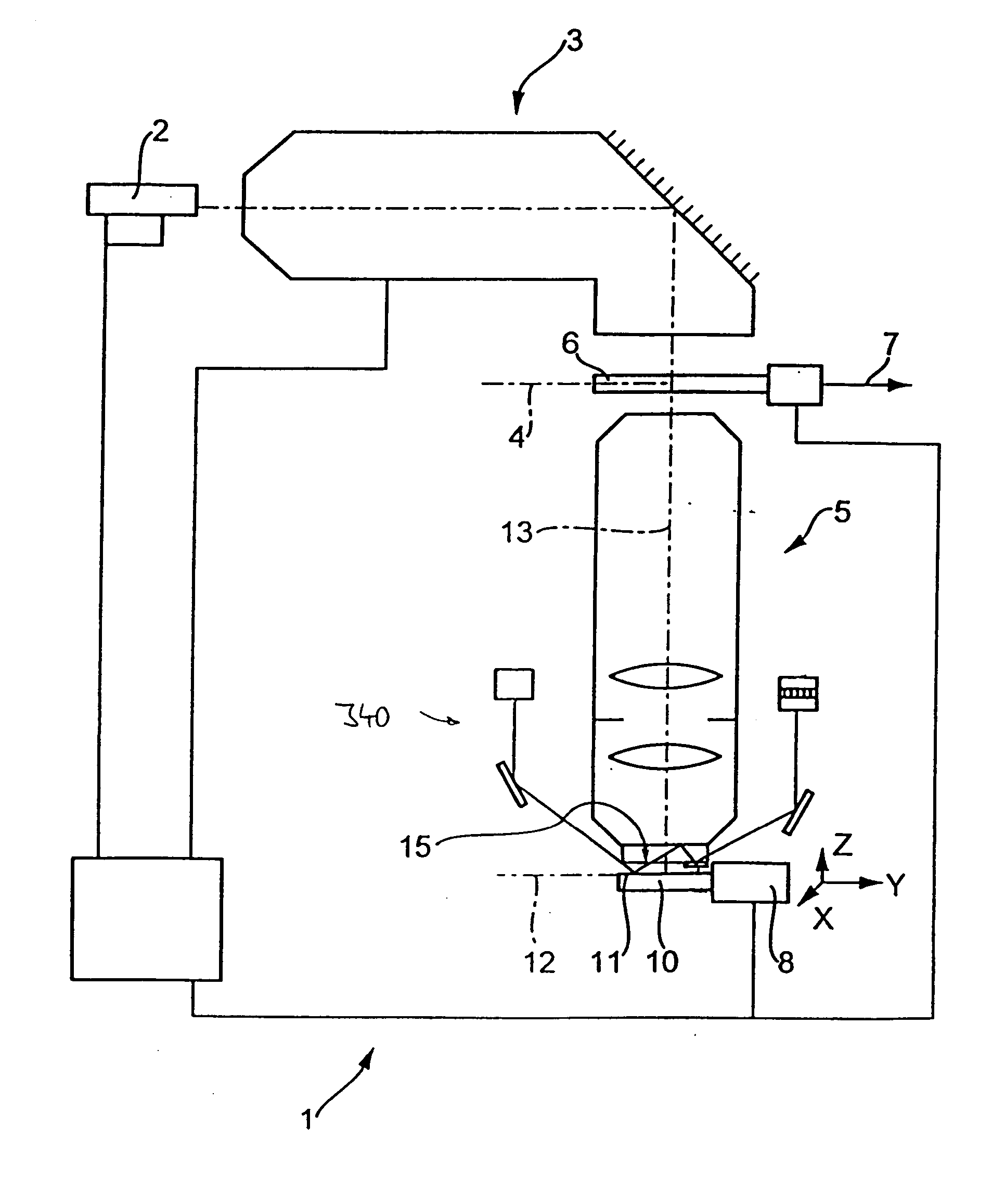
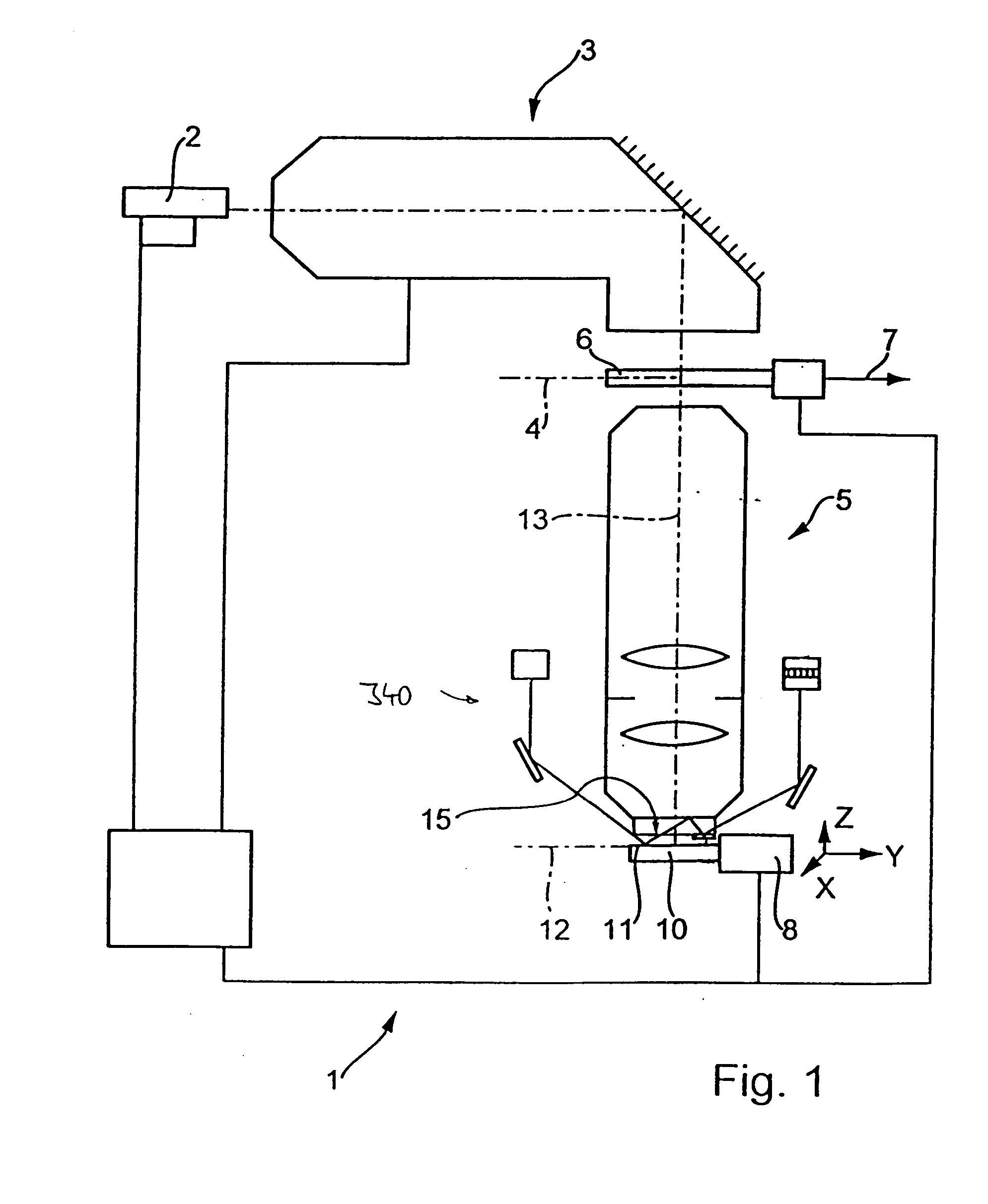
[0037]FIG. 1 shows a diagram of a microlithographic projection exposure machine in the form of a wafer stepper 1 which is provided for manufacturing highly integrated semiconductor devices. The projection exposure machine 1 comprises as light source an excimer laser 2 with an operating wavelength of 157 nm, other operating wavelengths, for example 193 nm or 248 nm also being possible. A downstream illuminating system 3 produces in its exit plane 4 a large, sharply delimited, very homogeneously illuminated image field which is adapted to the telecentric requirements of the downstream projection objective 5. The illuminating system 3 has devices for selecting the illuminating mode and in the example can be switched over between conventional illumination with a variable degree of coherence, ring-field illumination and dipole or quadrupole illumination. Arranged downstream of the illuminating system is a device for holding and manipulating a mask 6 such that the latter lies in the objec...


PUM


Abstract

In a method for manufacturing semiconductor devices and other finely structured parts, a projection objective (5) is used in order to project the image of a pattern arranged in the object plane of the projection objective onto a photosensitive substrate which is arranged in the region of the image plane (12) of the projection objective. In this case, there is set between an exit surface (15), assigned to the projection objective, for exposing light and an incoupling surface (11), assigned to the substrate, for exposing light a small finite working distance (16) which is at least temporarily smaller in size and exposure time interval than a maximum extent of an optical near field of the light emerging from the exit surface. As a result, projection objectives with very high numerical apertures in the region of NA>0.8 or more can be rendered useful for contactless projection lithography.

Description

[0001] This is a Continuation-In-Part Application of application Ser. No. 10 / 210,051, filed Aug. 2, 2002, which claims benefit of the German Patent Application No. 102 29 818.1 filed on Jun. 28, 2002, and is further a Continuation-In-Part Application of application Ser. No. 10 / 379,809 filed on Mar. 6, 2003, which claims benefit of the German Patent Application No. 102 10 899.4 filed on Mar. 8, 2002. The disclosures of application Ser. No. 10 / 210,051 and of application Ser. No. 10 / 379,809 are incorporated into this Continuation-In-Part-Application by reference. Benefit is further claimed of the German Patent Application No. 103 32 112.8 filed on Jul. 9, 2003, the disclosure of which is also incorporated by reference.BACKGROUND OF THE INVENTION [0002] 1. Field of the Invention [0003] The invention relates to methods for manufacturing semiconductor devices and other finely structured components, and to projection exposure systems for carrying out the methods. [0004] 2. Description of t...

Claims


Application Information

Patent Timeline
IPC IPC(8): G02B7/28G02B13/14G03F7/20G03F9/00
CPCB82Y10/00G02B7/28G03F9/7026G03F7/70325G03F7/70341G02B13/14
Inventor SCHUSTER, KARL-HEINZ
Owner CARL ZEISS SMT GMBH
Why Eureka
Try Eureka