
Wiring board, manufacturing method thereof, semiconductor device and manufacturing method thereof

Active Publication Date: 2005-02-24
SEMICON ENERGY LAB CO LTD
View PDF23 Cites 14 Cited by
  • Summary
  • Abstract
  • Description
  • Claims
  • Application Information

AI Technical Summary

Benefits of technology

[0008] In manufacturing steps of multi-layer wirings for the LSI development, at least two additional masking steps are required for every additional wiring. In addition, a planarization step or the like is required. The planarization step for an interlayer film is performed in order to suppress the change in width of wirings due to the stepped surface of the interlayer film as well as to improve an exposure accuracy in exposure steps. As for a planarization step for the LSI development for example, CMP (Chemical Mechanical Polishing) is applied after depositing a thick interlayer film. Alternatively, a method for performing etch back after depositing an interlayer film and a flat film in this order, or a combination of the etch back with the above CMP can be employed. However, when forming multi-layer wirings over a large substrate using these methods, it is quite difficult to deposit an interlayer film with uniform thickness and to obtain flatness. Furthermore, since flatness of an upper layer reflects flatness of a lower layer, the planarization becomes even more indispensable as the number of wirings is increased, which further increases the number of manufacturing steps. Accordingly, in the case of integrally forming a functional circuit and a display device on the same substrate, it is necessary that multi-layer wirings are achieved with a small number of steps in order to provide an inexpensive device.
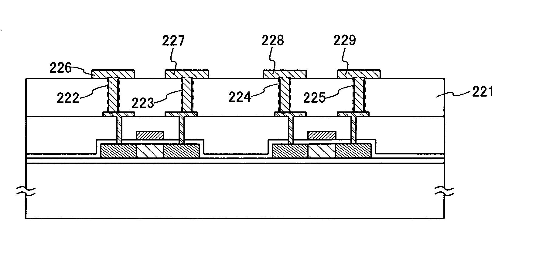
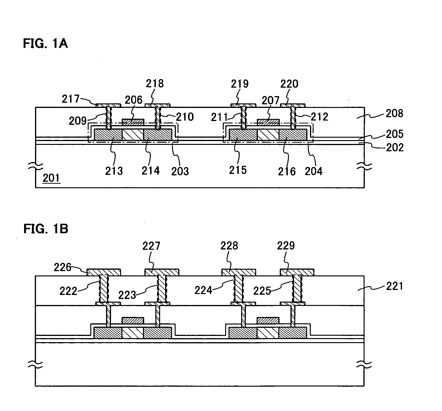
[0013] According to the above structure, the structure that the third wiring is wider than the first and second wirings while the second wiring is wider than the first wiring means that the wiring in the upper layer which is added later is formed wider than the wiring in the lower layer. By forming the wider wiring in the upper layer in this manner, an area occupied by the wiring in the lower layer can be reduced. In addition, by forming a wide wiring such as a power supply wiring in the upper layer, the contact hole in the upper layer can be formed larger than that in the lower layer.
[0020] Among the interlayer insulating films of the invention, at least one of them is formed of organic resin. An organic resin film has a lower dielectric constant than an inorganic film, which is typically used as an interlayer film. Therefore, parasitic capacitance can be reduced, leading to a higher operating rate of a functional circuit. In addition, since the interlayer insulating film containing organic resin has superior flatness at the time of deposition, a planarization step can be omitted. However, it is difficult to form a minute contact hole in an organic resin film in terms of the material characteristics in general. According to the invention, a larger contact hole can be formed in the upper layer, therefore, less restrictive conditions are given on microfabrication, and thus organic resin can be effectively used for an interlayer insulating film.
[0032] Among the interlayer insulating films of the invention, at least one of them may contain organic resin. An organic resin film has a lower dielectric constant than an inorganic film which is typically used as an interlayer film. Therefore, parasitic capacitance can be reduced. In addition, since the interlayer insulating film using organic resin is superior in flatness at the time of deposition, a planarization step can be omitted, leading to a higher operating rate of a functional circuit. However, it is difficult to form a minute contact hole in an organic resin film in terms of the material characteristics in general. According to the invention, the contact hole in the upper layer can be formed large in diameter, therefore, less restrictive conditions are given on the microfabrication, and thus organic resin can be effectively used for an interlayer insulating film.
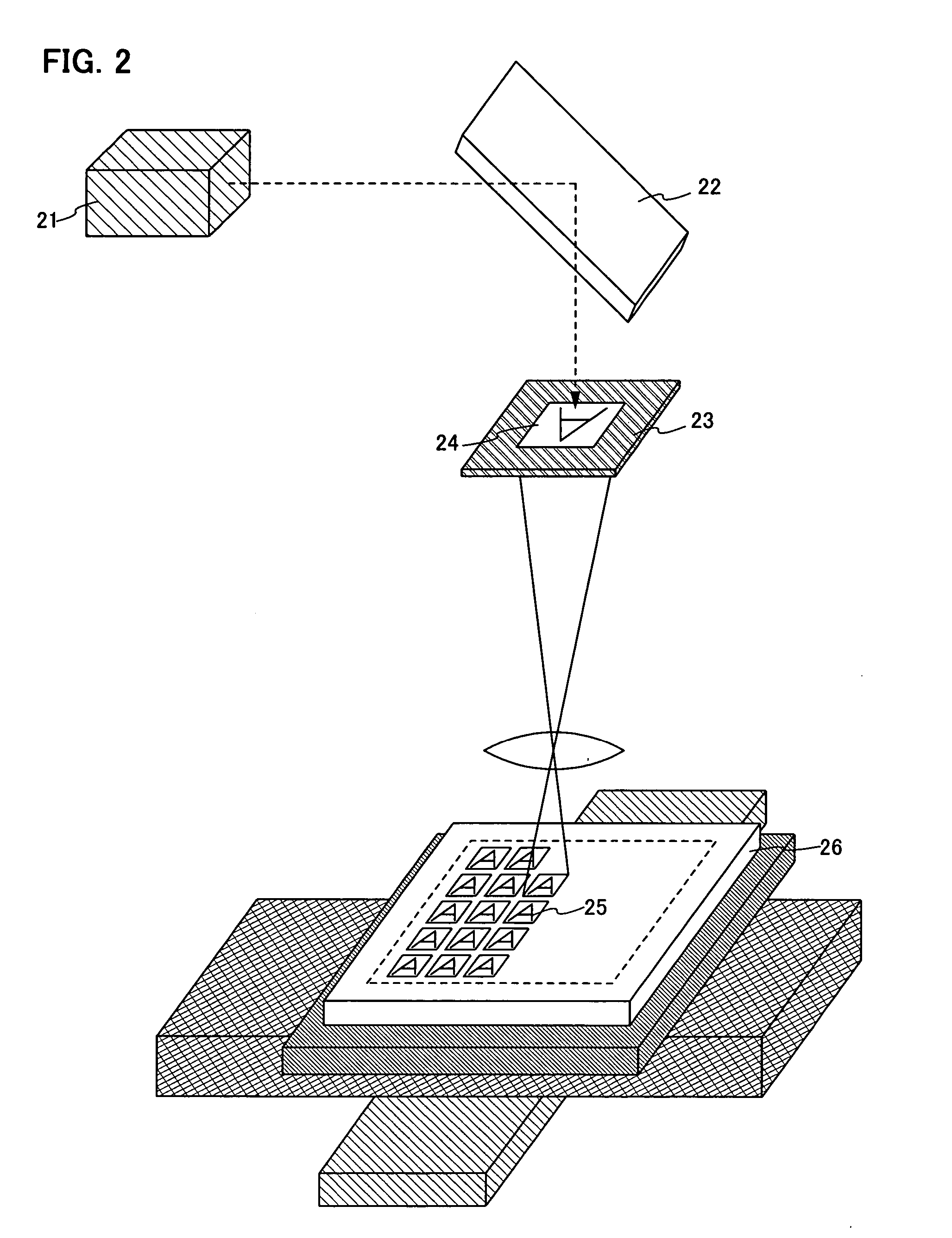
[0038] According to the manufacturing method of a wiring board having the above structure, the exposure system which is different from the rest of the exposure systems is a system which can apply exposure with a higher resolution, a higher accuracy of position and in a narrower range of exposure as compared to the rest of the exposure systems.
[0048] According to the semiconductor device and the manufacturing method thereof of the invention, a planarization step as one of the additional steps that are required accompanied by the increased number of the wiring layers can be omitted or drastically simplified. Therefore, a multi-layer wiring of a functional circuit can be achieved at low cost. By the achievement of the multi-layer wiring, the layout area of the functional circuit can be reduced, leading to a higher operating rate and higher performance of the functional circuit. In addition, since an exposure system capable of applying exposure in a wide range can be used as the exposure system for forming the wiring in the upper layer, a functional circuit and a display device can be efficiently integrated over a large substrate. Accordingly, a high-performance functional circuit or a display device having the high-performance functional circuit can be provided inexpensively.

Problems solved by technology

However, when forming multi-layer wirings over a large substrate using these methods, it is quite difficult to deposit an interlayer film with uniform thickness and to obtain flatness.

Method used


Image

  • Wiring board, manufacturing method thereof, semiconductor device and manufacturing method thereof
  • Wiring board, manufacturing method thereof, semiconductor device and manufacturing method thereof
  • Wiring board, manufacturing method thereof, semiconductor device and manufacturing method thereof

Examples


embodiment 1

[0086] [Embodiment 1]

[0087] Described now is an embodiment with reference to FIGS. 5 and 6. FIG. 5 is a top view showing an example of a mask layout of a structure of the functional circuit of the invention. FIG. 6 is a part of a cross-sectional view of FIG. 5 taken along lines A-B and B-C. In FIG. 5, a channel forming region, a source region, and a drain region of each TFT are formed in a semiconductor layer 501. A gate wiring 507 and a wiring 508 between TFTs correspond to a first wiring. The first contact hole 503 electrically connects the first wiring to the second wiring or an active layer to the second wiring. A wiring 509 between TFTs, a power supply wiring 510 and a ground wiring 511 correspond to a second wiring 504. The second contact hole 505 electrically connects the second wiring to the third wiring. A power supply wiring 512 and a ground wiring 513 correspond to a third wiring 506.

[0088] Lead wirings of TFTs in the functional circuit are formed by the first wiring 502...

embodiment 2

[0092] [Embodiment 2]

[0093] Described with reference to FIGS. 4A and 4B now is a different embodiment from Embodiment 1. In this embodiment, a panel in which a display portion, driver circuits for controlling the display portion, a memory and a CPU on the same surface is described. FIG. 4A is a top plan view of a panel which is formed by sealing liquid crystal with a TFT substrate and a counter substrate and a sealant. FIG. 4B is a cross-sectional view of FIG. 4A taken along a line A-A′.

[0094]FIG. 4A is an external view of a panel including a pixel portion 701 in which multiple pixels are arranged in matrix over a substrate 700. Around the pixel portion 701, a signal line driver circuit 702 and a scan line driver circuit 703 for controlling the pixel portion 701 are disposed. A sealant 707 is provided so as to surround all of them. A counter substrate 709 may be provided over only the pixel portion 701, the signal line driver circuit 702 and the scan line driver circuit 703, or ove...

embodiment 3

[0102] [Embodiment 3]

[0103] Described in this embodiment with reference to FIGS. 7A to 7G are examples of electronic apparatuses which are manufactured according to the invention.

[0104] Electronic apparatuses manufactured according to the invention include a video camera, a digital camera, a goggle type display (head mounted display), a navigation system, a sound reproducing device (car audio set, component stereo and the like), a laptop personal computer, a video game machine, a portable information terminal (mobile computer, mobile phone, portable game machine and the like), an image reproducing device provided with a recording medium (specifically, a device reproducing a recording medium such as a DVD (Digital Versatile Disc) and displaying the reproduced image) and the like. Specific examples of these electronic apparatuses are shown in FIGS. 7A to 7G.

[0105]FIG. 7A is a display device including a housing 1401, a supporting base 1402, a display portion 1403 and the like. The in...


PUM


Abstract

The invention provides a wiring board having a small-scale and high-performance functional circuit while realizing a multi-layer wiring with a small number of steps. In addition, the invention provides a semiconductor device in which a display device is integrated with such high-performance functional circuit on the same substrate. According to the invention, first to third wirings, first and second interlayer insulating films and first and second contact holes are formed over a substrate having an insulating surface. The second wiring is wider than the first wiring, or the third wiring is wider than the first wiring or the second wiring. The second contact hole has a larger diameter than the first contact hole.

Description

BACKGROUND OF THE INVENTION [0001] 1. Field of the Invention [0002] The present invention relates to a multi-layer wiring board and a manufacturing method thereof. In addition, the invention relates to a semiconductor device using the multi-layer wiring board and a manufacturing method thereof. [0003] 2. Description of the Related Art [0004] In recent years, semiconductor devices formed by using TFTs (Thin Film Transistors) that includes polycrystalline semiconductor thin films as switching elements for a pixel portion or pixel driver circuits are actively studied and developed. Since such TFTs including polycrystalline semiconductor thin films have the advantages of high field effect mobility and the like, technologies for integrally forming a display device and a functional circuit on the same substrate are also under research and development. As for functional circuits, there are CPUs, image signal processing circuits, memories and the like. In order to improve a value of a semic...

Claims


Application Information

Patent Timeline
IPC IPC(8): H01L21/4763H01L21/48H01L21/60H01L21/768H01L21/77H01L23/14H01L23/48H01L23/482H01L27/12H05K1/00H05K3/46
CPCH01L21/76838H01L23/4824H01L27/12H01L27/1277H01L2924/0002H01L27/124H01L2924/00
Inventor KUROKAWA, YOSHIYUKI
Owner SEMICON ENERGY LAB CO LTD
Learn More