Atomic layer deposition of metallic contacts, gates and diffusion barriers

Active Publication Date: 2005-02-24
GLOBALFOUNDRIES US INC
View PDF11 Cites 102 Cited by
  • Summary
  • Abstract
  • Description
  • Claims
  • Application Information

AI Technical Summary

Benefits of technology

[0025] It is noted that the low temperature thermal ALD method and the PE-ALD method of the present invention can provide metallic films with high conformality, low growth-temperatures, low impurity content, minimal dielectric damage and little or no silicon consumption. With respect to the impurity content, the methods of the present invention can form metallic films that have an impurity content of about 1% or less, with an impurity content of about 0.5 % or less being more typical.
[0026] The methods of the present invention can be used to form graded compo

Problems solved by technology

For this, the sputtering of TaSixNy films is not an adequate technique since sputtering typically does not provide sufficient conformality.
Thus, the sputtering mechanism makes it difficult to provide highly conformal diffusion barriers in high aspect

Method used


Image

  • Atomic layer deposition of metallic contacts, gates and diffusion barriers
  • Atomic layer deposition of metallic contacts, gates and diffusion barriers
  • Atomic layer deposition of metallic contacts, gates and diffusion barriers

Examples


Example

EXAMPLE 1

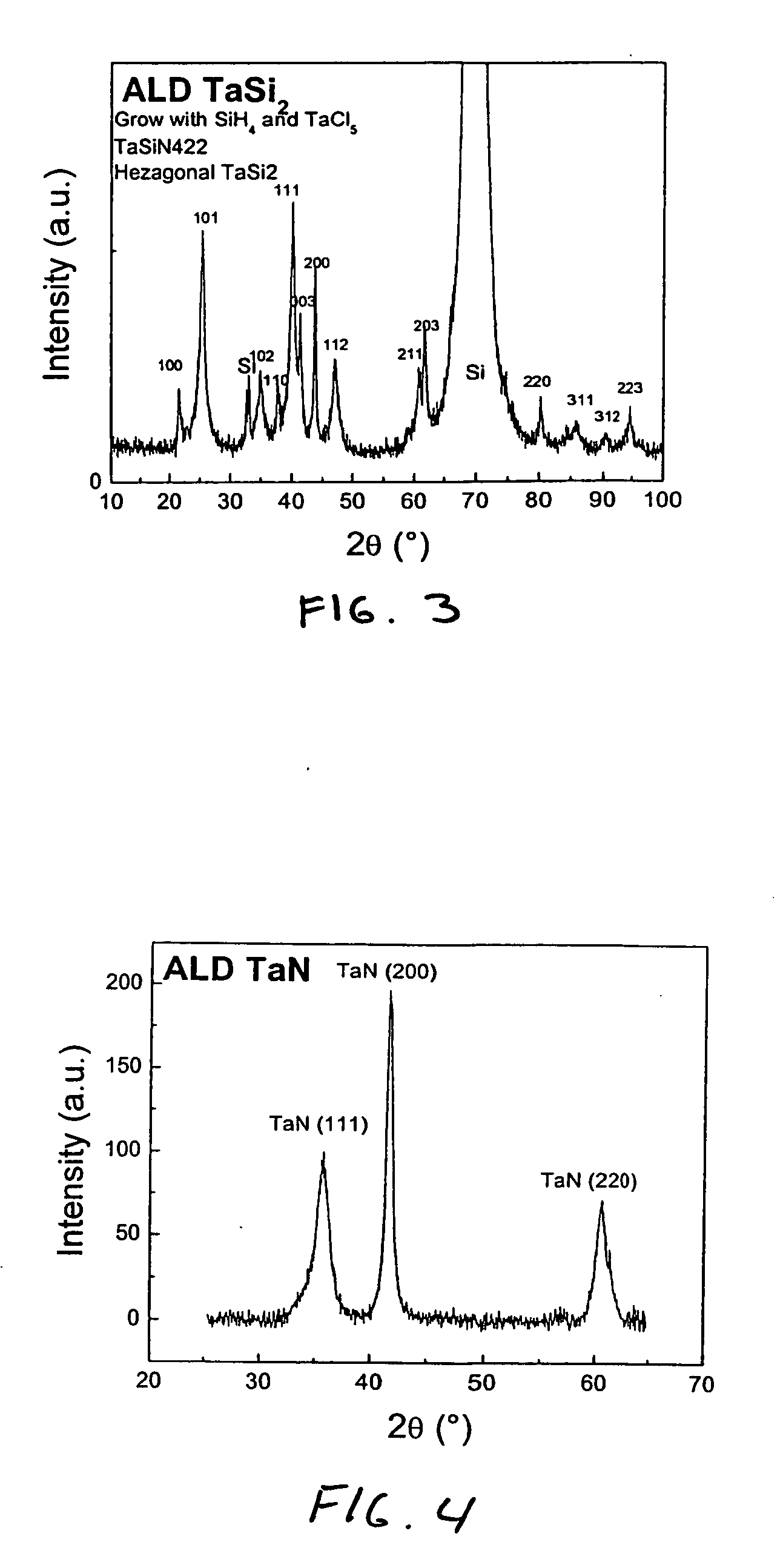
[0068] Atomic Layer Deposition of TaSi2

[0069] For this experiment, an atomic layer deposition chamber was used. Samples sizes as large as 200 nm diameter could be loaded with the atomic layer deposition chamber. After the sample was loaded, the chamber was pumped by a reactive gas turbo molecular pump with a working base pressure of 10−6 Torr. The sample heating was performed using a ceramic resistive heating plate, providing growth temperatures up to 450° C. The temperature was controlled by varying current to the heater, which was previously calibrated against a thermocouple attached to a sample.

[0070] Solid TaCl5 (powder) contained in a glass tube was used as the metal precursor. The glass tube was maintained at 100° C. to develop adequate vapor pressure and all the delivery lines were heated between 130°−150° C. to prohibit condensation of the precursor. To improve the delivery, Ar was used as a carrier gas and the flow was controlled by a leak valve upstream from th...

Example

EXAMPLE 2

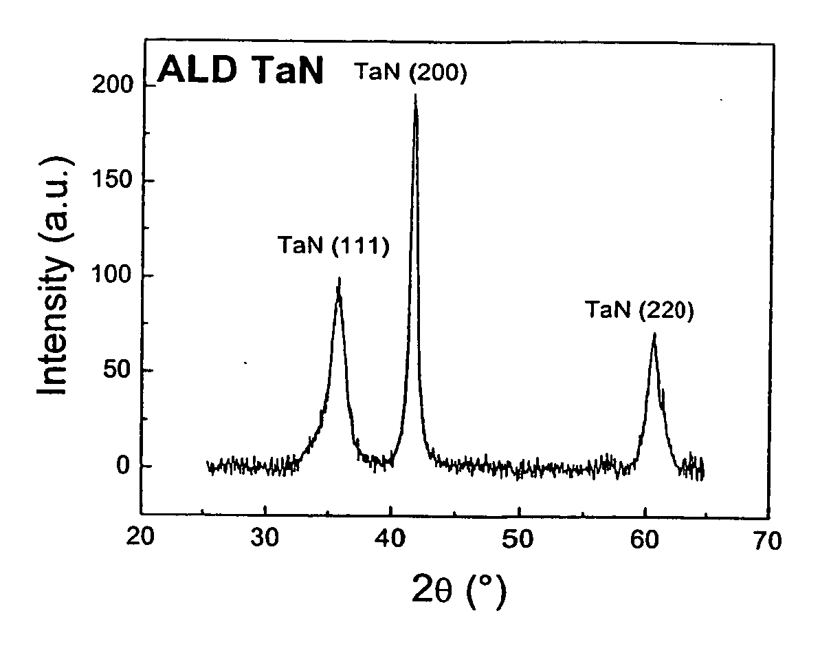
[0073] Atomic Layer Deposition of TaSiN

[0074] For this experiment, a plasma-enhanced atomic layer deposition chamber was used. Samples sizes as large as 200 nm diameter could be loaded with the atomic layer deposition chamber. After the sample was loaded, the chamber was pumped by a reactive gas turbo molecular pump with a working base pressure of 10−6 Torr. The sample heating was performed using a ceramic resistive heating plate, providing growth temperatures up to 450° C. The temperature was controlled by varying current to the heater, which was previously calibrated against a thermocouple attached to a sample.

[0075] Solid TaCl5 (powder) contained in a glass tube was used as the metal precursor. The glass tube was maintained at 100° C. to develop adequate vapor pressure and all the delivery lines were heated between 130°−150° C. to prohibit condensation of the precursor. To improve the delivery, Ar was used as a carrier gas and the flow was controlled by a leak valve u...


PUM


Abstract

The present invention provides metallic films containing a Group IVB or VB metal, silicon and optionally nitrogen by utilizing atomic layer deposition (ALD). In particularly, the present invention provides a low temperature thermal ALD method of forming metallic silicides and a plasma-enhanced atomic layer deposition (PE-ALD) method of forming metallic silicon nitride film. The methods of the present invention are capable of forming metallic films having a thickness of a monolayer or less on the surface of a substrate. The metallic films provided in the present invention can be used for contact metallization, metal gates or as a diffusion barrier.

Description

FIELD OF THE INVENTION [0001] The present invention relates to the fabrication of a metallic film, and more particularly to the formation of a metallic film using atomic layer deposition (ALD). The metallic films that are formed in the present invention can be used for contact metallization, a metal gate or as a conductive diffusion barrier depending upon the elements present in the metallic film as well as the materials surrounding the metallic film. In particular, the present invention provides a plasma enhanced ALD method and a low temperature thermal ALD method for fabricating conformal metallic films having a thickness of about 100 Å or less on a surface of a substrate. BACKGROUND OF THE INVENTION [0002] In the semiconductor industry, TaSixNy films have been extensively studied as a barrier layer for Cu interconnects and as a bottom electrode for DRAM capacitors. Such films typically exhibit low resistivity and excellent thermal / chemical stability against high temperature proce...

Claims


Application Information

Patent Timeline
IPC IPC(8): H01L21/28H01L21/285H01L21/3205H01L21/768H01L29/49
CPCH01L21/28088H01L21/28562H01L2221/1078H01L21/76841H01L29/4966H01L21/32053
Inventor CABRAL, CYRIL JR.KIM, HYUNGJUNROSSNAGEL, STEPHEN M.
Owner GLOBALFOUNDRIES US INC
Why Eureka
Try Eureka