Transparent error correcting memory

a technology of error correction and memory, applied in the field of error detection and correction in memory, can solve the problems of soft errors, hard errors, and defects in semiconductor devices, and achieve the effect of not increasing the write access time of memory devices

Inactive Publication Date: 2005-02-24
MOSYS INC
View PDF87 Cites 58 Cited by
  • Summary
  • Abstract
  • Description
  • Claims
  • Application Information

AI Technical Summary

Benefits of technology

[0011] Accordingly, the present invention provides a memory device or an embedded memory block that includes an array of memory cells with built-in ECC protection. In one embodiment, the memory cells are DRAM cells. In another embodiment, the memory cells are SRAM cells. Th

Problems solved by technology

Semiconductors memories such as DRAM and SRAM devices are susceptible to both soft and hard errors.
Soft errors are generated when sub-atomic energetic particles hit the memory device and generate charge high enough to upset the state of one or more memory cells.
Hard errors are generated by defects in the semiconductor device during the manufacturing process.
This, however, is accomplished at the cost of larger area.
As a result, the error correction scheme does not increase the read latency of the memory.
As a result, the generation of error correction check bits does not increase the write latency of the memory.
However, this error correction scheme cannot correct data errors occurring in the first read operation of a burst read sequence, or in data written to the memory before the error correction check bits are generated.
In addition, even though delays through the I/O circuit are eliminated, the delays through the ECC correction circuit still increase the memory cycle time.
The addition of ECC storage and circuitry complicates memory testing.
In the embedded environment, where error-correction is hidden from the application, the ECC bits cannot be directly accessed for testing.
The chance of havin

Method used


Image

  • Transparent error correcting memory
  • Transparent error correcting memory
  • Transparent error correcting memory

Examples


Embodiment Construction

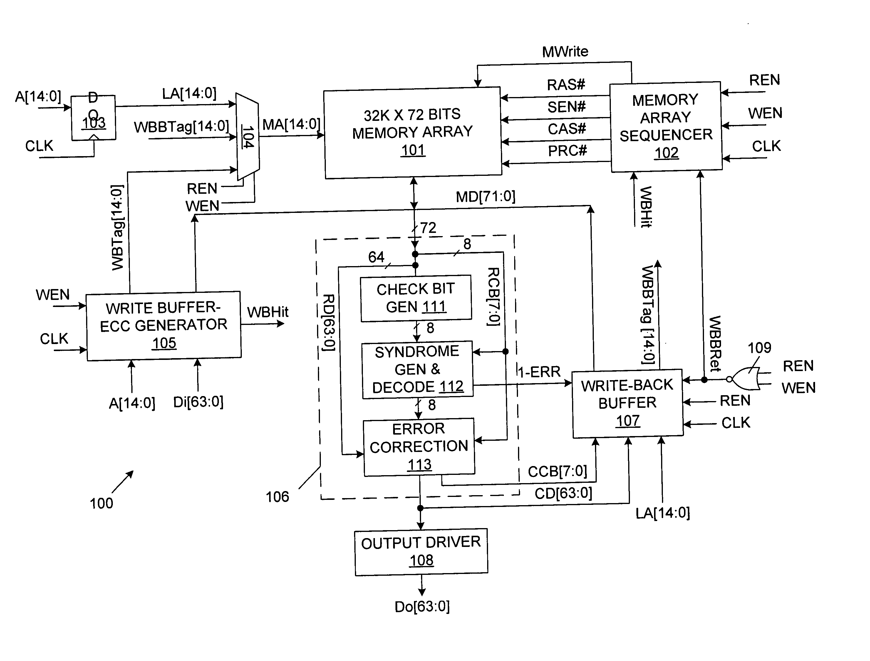
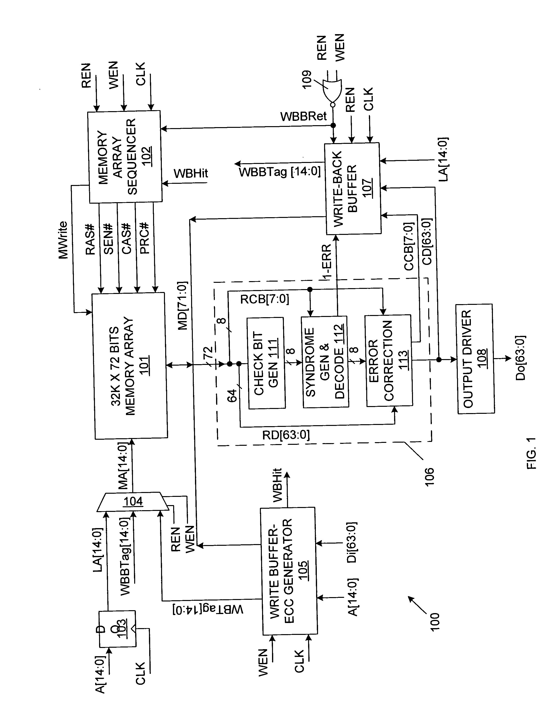
[0029]FIG. 1 is a block diagram of a memory device 100 in accordance with one embodiment of the present invention. Memory device 100 includes memory array 101, memory array sequencer 102, address register 103, multiplexer 104, write buffer / ECC generator 105, error detection / correction circuit 106, write-back buffer 107, output driver 108 and NOR gate 109. The external interface of memory device 100 includes a 64-bit input data bus Di[63:0], a 64-bit output data bus Do[63:0], a read enable line REN, a write enable line WEN, a clock line CLK, and a 15-bit address bus A[14:0]. In the described embodiments, each bus / line and the corresponding signal are identified using the same reference element. For example, Di[63:0] is used to identify both the input data bus and the input data value transmitted on the input data bus.

[0030] In the described example, memory array 101 is a conventional 32 k×72-bit memory array, although this is not necessary. In the described embodiment, memory array ...


PUM


Abstract

A memory system with transparent error correction circuitry provides full stuck-at fault coverage for both test data patterns and the corresponding error correction code (ECC) values. The memory system includes a semiconductor memory having a memory array, a memory interface and an error detection/correction unit. The memory array is configured to store test data patterns and corresponding error correction code (ECC) values. The memory interface is configured such that the ECC values are not directly accessible. The error detection/correction unit is configured to correct single-bit errors in the test data patterns and corresponding ECC values. A set of test data patterns associated with the semiconductor memory is selected such that any multiple-bit error in a test data pattern and the corresponding ECC value causes the error detection/correction unit to provide an output data pattern having an error, thereby rendering multiple-bit faults 100% detectable.

Description

RELATED APPLICATIONS [0001] This is a continuation in part of Pending U.S. patent application Ser. No. 10 / 003,602, “Error Correcting Memory And Method of Operating Same” by Wingyu Leung and Fu-Chieh Hsu. The present invention is also related to U.S. Pat. No. 6,147,535, entitled “Clock Phase Generator for controlling operation of a DRAM Array” by Wingyu Leung.FIELD OF THE INVENTION [0002] The present invention relates to semiconductor memory systems, such as static random access memory (SRAM) systems or dynamic random access memory (DRAM) systems. In particular, the present invention relates to a method and apparatus of error detection and correction in a semiconductor memory that works with on-chip built-in-self-test logic. The present invention is particularly applicable to embedded fault-tolerant memory, which incorporates error-correction circuitry (ECC) for both soft and hard error correction. DISCUSSION OF RELATED ART [0003] Semiconductors memories such as DRAM and SRAM devices...

Claims


Application Information

Patent Timeline
IPC IPC(8): G06F11/10
CPCG06F11/1048
Inventor LEUNG, WINGYUTAM, KIT SANGTWOREK, MIKOLAJHSU, FU-CHIEH
Owner MOSYS INC
Why Eureka
Try Eureka