Integrated circuit chip with improved array stability

a technology of array stability and integrated circuits, which is applied in the field of integrated circuit chips, can solve the problems of increasing chip power consumption, increasing cooling and packaging costs, and complex fets, so as to improve static random access memory (sram) cell stability, improve sram stability, and reduce sram cell leakage

Inactive Publication Date: 2005-03-24
MICROSOFT TECH LICENSING LLC
View PDF11 Cites 32 Cited by
  • Summary
  • Abstract
  • Description
  • Claims
  • Application Information

AI Technical Summary

Benefits of technology

[0009] It is a purpose of the invention to improve static random access memory (SRAM) cell stability;
[0010] It is another purpose of the invention to reduce SRAM cell leakage;
[0011] It is yet another purpose of the invention to improve SRAM stability and reduce leakage while minimizing performance degradation;
[0012] It is yet another purpose of the invention to improve SRAM stability and reduce leakage while minimizing performance degradation in PD SOI CMOS SRAMs;
[0013] It is yet another purpose of the invention to improve SRAM stability on PD SOI CMOS IC chips while reducing PD SOI CMOS IC chip leakage.
[0014] The present invention relates to a multi-thres

Problems solved by technology

Thus, not withstanding the decrease of chip supply voltage, chip power consumption has increased as well.
Both at the chip and system levels, cooling and packaging costs have escalated as a natural result of this increase in chip power.
In practice, typical FETs are much more complex than switches and transient power for circuit loads accounts for only a portion of CMOS chip power consumption.
This is especially true in what is known as partially depleted (PD) or fully depleted (FD) silicon on insulator (SOI) technologies, where subthreshold leakage has been shown to increase dramatically, such that it may be the dominant source of leakage.
When multiplied by the millions and even billions of devices on a state of the art SRAM, even 100 picoAmps (100 pA) of leakage in each of a million cells, for example, results in chip leakage on the order of 100 milliAmps (100 mA).
It has become especially difficult to scale gate dielectric simply because gate dielectric thickness is reaching its limit.
At a few mono-layers of Silicon, for example, deposition non-uniformity causes pinholes and diel

Method used


Image

  • Integrated circuit chip with improved array stability
  • Integrated circuit chip with improved array stability
  • Integrated circuit chip with improved array stability

Examples


Embodiment Construction

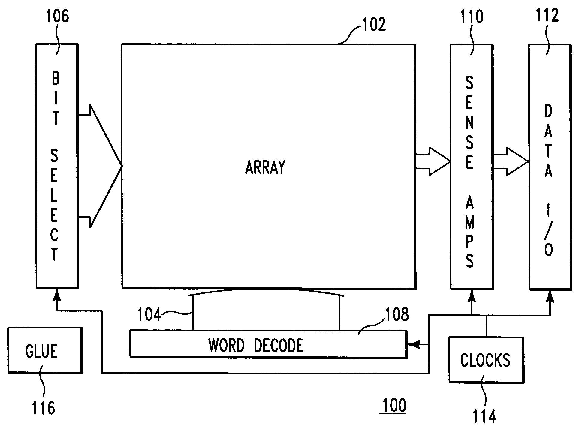
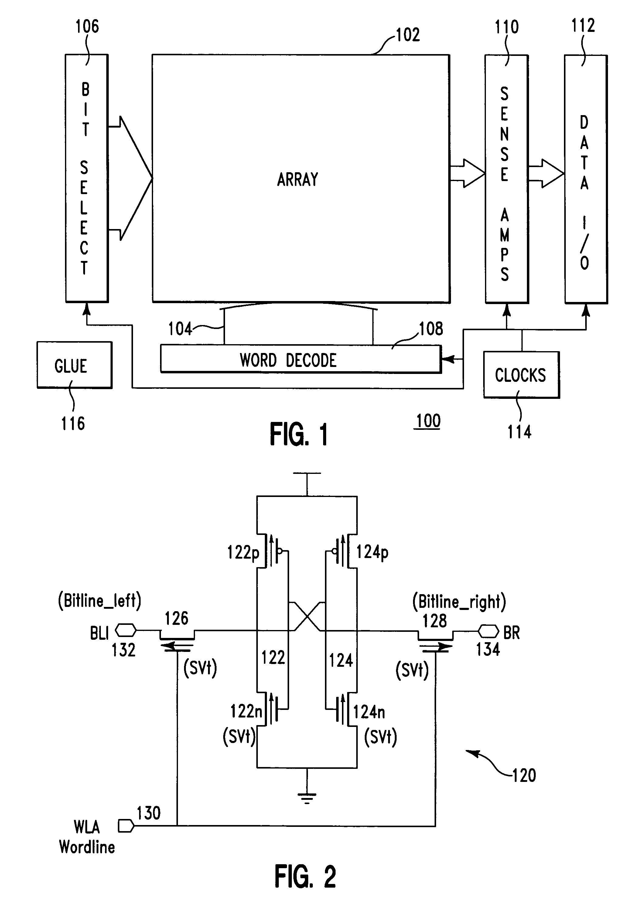
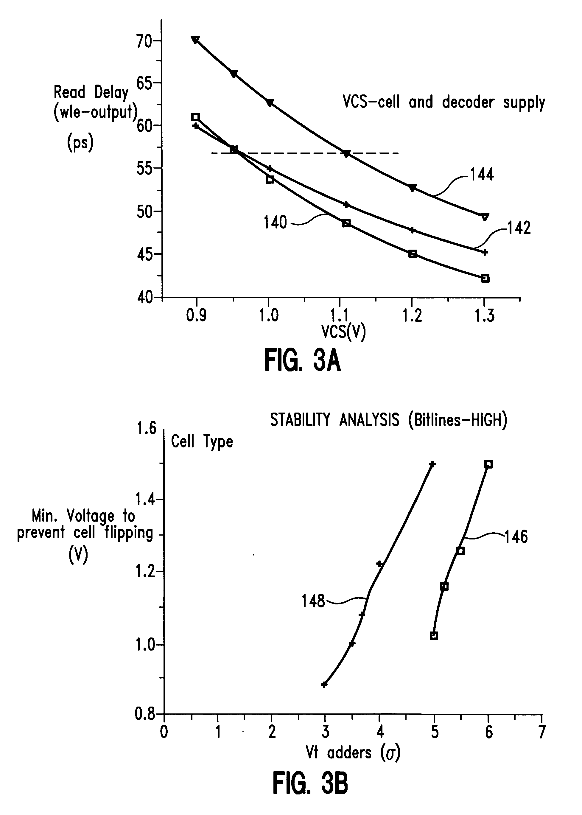
[0019] Turning now to the drawings and, more particularly, FIG. 1 shows a multi-threshold CMOS (MTCMOS) storage circuit 100 (e.g., memory), macro or chip, according to a preferred embodiment of the present invention. Preferably, the chip is supplied with multiple supply voltages with at least one increased supply that is provided to selected circuits or portions of circuits, e.g., the array 102 and selected support circuits, such as word line drivers 104. Selected devices or field effect transistors (FETs) in those circuits 102, 104 are tailored to reduce leakage current and to be resistant to increased leakage from bias conditions. In particular, support circuit FETs in the storage circuit have a base device design threshold (VT) that is typical for the base technology and horizontally equivalent tailored FETs (i.e., same design length and width) have a higher threshold voltage (VT+), e.g., from thicker gate oxide and channel doping for reduced subthreshold leakage. Individual func...


PUM


Abstract

A multi-threshold integrated circuit (IC) that may be supplied by multiple supplies, with an array of latches such as an array static random access memory (SRAM) cells and a CMOS SRAM with improved stability and reduced subthreshold leakage. Selected devices (NFETs and/or PFETs) in array cells and support logic, e.g., in the data path and in non-critical logic, are tailored for lower gate and subthreshold leakage. Normal base FETs have a base threshold and tailored FETs have a threshold above. In a multi-supply chip, circuits with tailored FETs are powered by an increased supply voltage.

Description

CROSS REFERENCE TO RELATED APPLICATION [0001] The present invention is a continuation in part of U.S. patent application Ser. No. 10 / 306,938, entitled “Storage Array Such As A SRAM with Reduced Power Requirements” to Joshi, published as US 2004 / 0105299 A1 and U.S. application Ser. No. 10 / 307,168, entitled “Reduced Integrated Circuit Chip Leakage and Method of Reducing Chip Leakage” to Chuang et al., published as US 2004 / 0105300 A1, both filed Nov. 29, 2002 and published Jun. 3, 2004 and is related to U.S. patent application Ser. No. 10 / 644,211, entitled “Method Of Reducing Leakage Current In Sub One Volt SOI Circuits” to Richard B. Brown et al., filed Aug. 22, 2003, all assigned to the assignee of the present invention.FIELD OF THE INVENTION [0002] The present invention is related to integrated circuit (IC) chips and more particularly to improving static random access memory (SRAM) stability while reducing IC power consumption. BACKGROUND DESCRIPTION [0003] Semiconductor technology ...

Claims


Application Information

Patent Timeline
IPC IPC(8): G11C5/06G11C8/08G11C11/00G11C11/413
CPCG11C8/08G11C11/413G11C11/412G11C11/417
Inventor CHAN, YUEN H.JOSHI, RAJIV V.PLASS, DONALD W.
Owner MICROSOFT TECH LICENSING LLC
Why Eureka
Try Eureka