SOI by oxidation of porous silicon

a technology of porous silicon and substrate structure, applied in the direction of semiconductor devices, vacuum evaporation coatings, coatings, etc., can solve the problems of difficult to form soi structures, inability to meet the requirements of the substrate, so as to achieve the effect of simple and cost-effective

Inactive Publication Date: 2005-03-31
GLOBALFOUNDRIES INC
View PDF20 Cites 55 Cited by
  • Summary
  • Abstract
  • Description
  • Claims
  • Application Information

AI Technical Summary

Benefits of technology

[0010] One object of the present invention is to provide a simple and cost effective method of fabricating silicon-on-insulator (SOI) substrate structures.
[0011] Another object of the present invention is to provide a method of fabricating SOI substrate structures in which the defect level is reduced by reducing implantation damages and by reducing the oxidation-induced stress and strain.
[0012] A further object of the present invention is to provide a simple and cost effective method of fabricating SOI substrate structures that are scalable to 300 mm.
[0014] These and other objects and advantages are achieved by utilizing a method in which the SOI substrate structure is fabricated by oxidation of graded porous Si. The graded porous Si has a relatively coarse top layer and a fine porous layer that is buried beneath the top layer. Upon a subsequent oxidation step, the fine buried porous layer is converted into a buried oxide, while the coarse top layer coalesces into a solid Si-containing over-layer by surface migration of Si atoms. Much of this top Si layer becomes thermal oxide, which can be easily removed, leaving only a thin Si over-layer above the buried oxide.
[0015] When a blanket implantation is used in the method of the present invention, the graded porous Si is spatially uniform laterally on the surface of a Si-containing substrate, and, as the oxidation occurs uniformly from all areas of the surface, the buried oxide is uniform and the Si over-layer is relatively stress free.
[0016] The method of the present invention provides several added benefits over the conventional SIMOX method mentioned above. One such benefit is that costly high-current implanters are not employed. A related benefit is the reduction of the implantation-induced damages. Additionally, the oxidation-induced stress and strain is less because the porous Si expands less in volume than does bulk Si upon oxidation.

Problems solved by technology

In fact, electrical and electronic coupling between the top device layer and the bulk can be, in some instances, quite deleterious.
However, forming SOI structures is no simple matter.
However, impurities at the bonded interface and the difficulty in achieving a thin, uniform Si over-layer through the etch-back process are major drawbacks.
With the Si substrate scaling up to larger wafer sizes, the high-cost of scaled-up high-current implanters and the implantation process itself is becoming a serious issue.
The actual structure of the porous Si, however, is a very complicated function of the type and concentration of dopants and defects, in addition to the above-mentioned parameters.
The presence of this large surface area makes porous Si very susceptible to chemical reaction with an ambient gas such as oxygen.
Although the oxidized porous Si provides good isolation, it is typically too thick relative to the Si islands and laterally non-uniform.
This non-uniformity leads to warping of the Si wafer and formation of many oxidation-induced defects in the Si islands.

Method used


Image

  • SOI by oxidation of porous silicon
  • SOI by oxidation of porous silicon
  • SOI by oxidation of porous silicon

Examples


Embodiment Construction

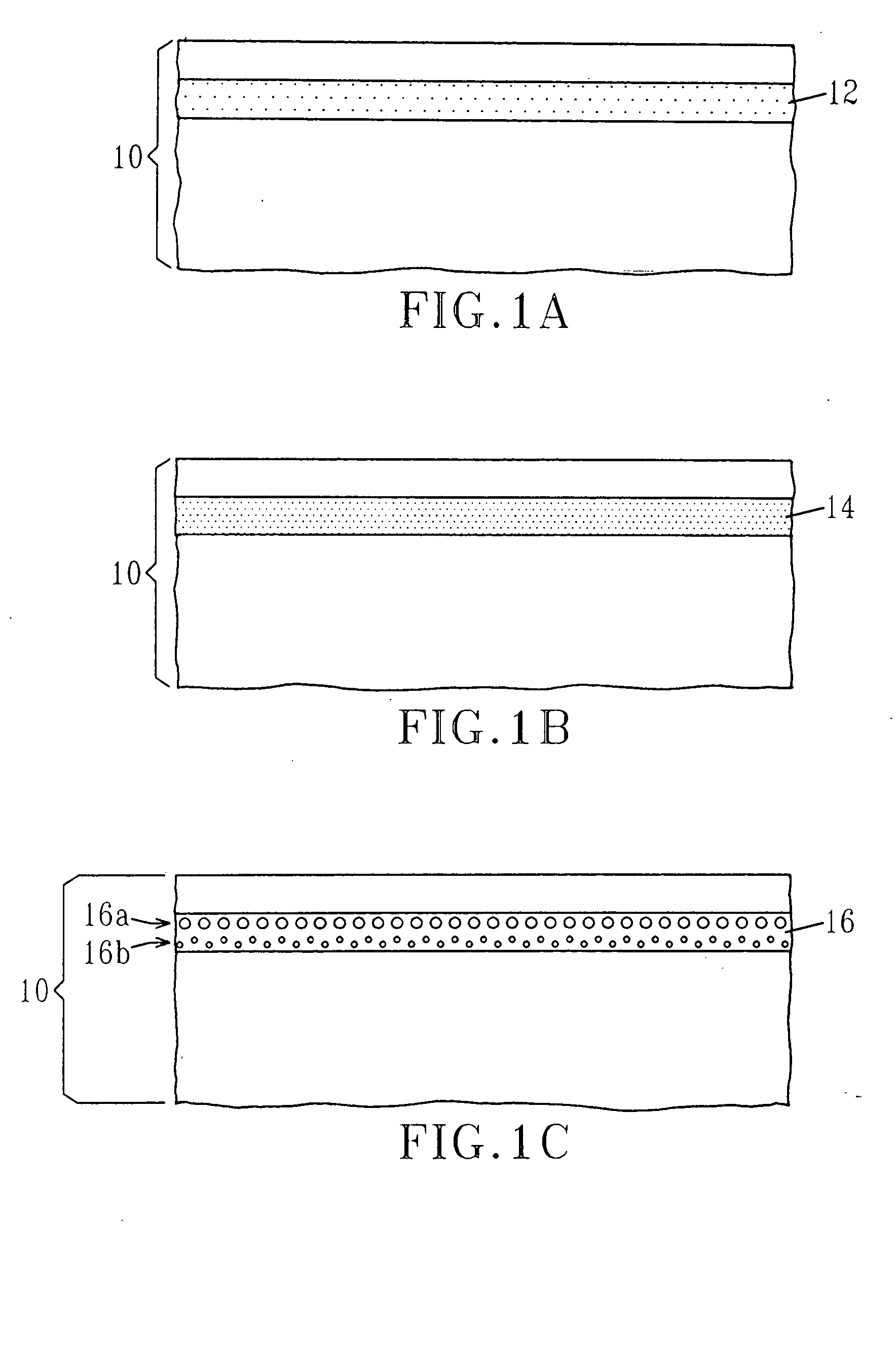
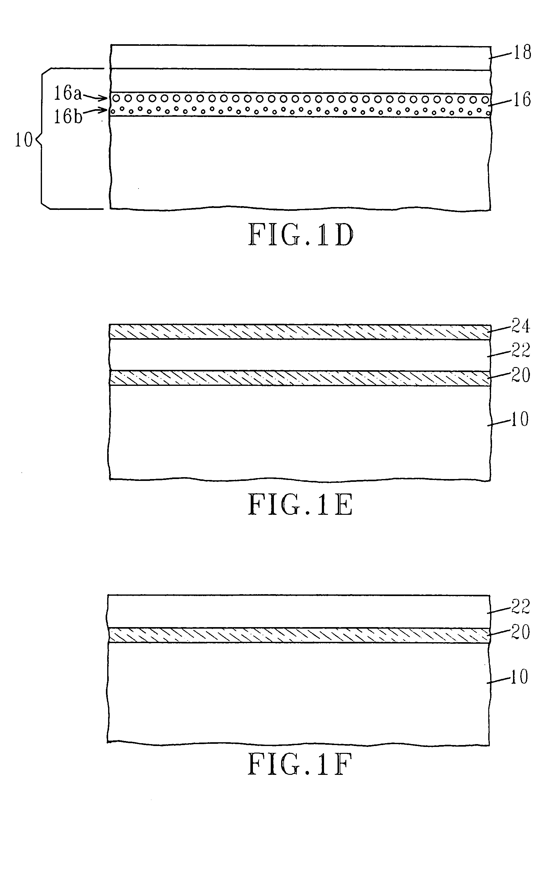
[0034] The present invention, which provides a simple and low-cost method for forming an SOI substrate structure having a uniform buried oxide layer underneath a Si-containing over-layer, will now be described in greater detail by referring to the drawings that accompany the present application. In the accompanying drawings, like and / or corresponding elements are referred to by like reference numerals.

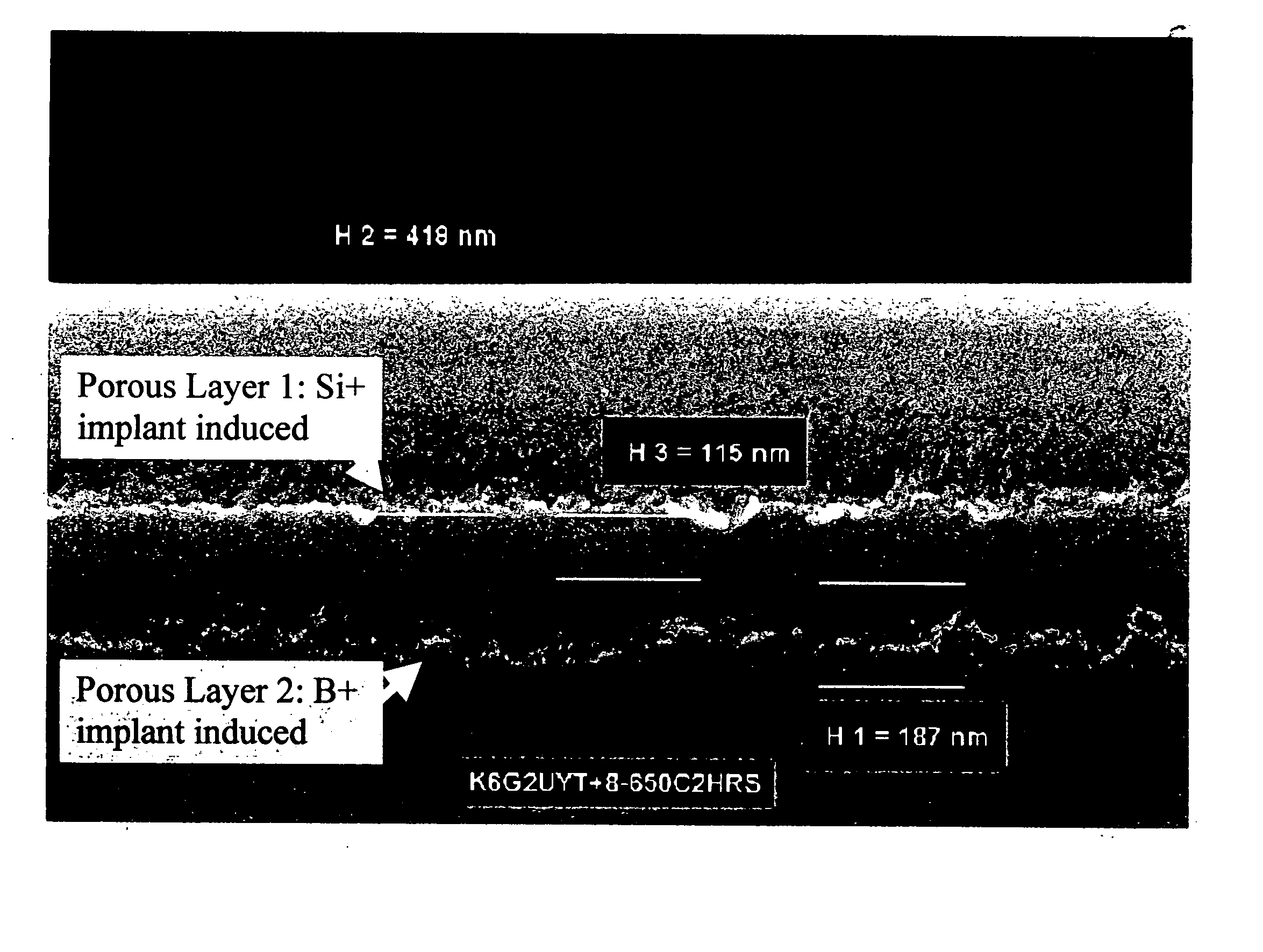
[0035] Reference is first made to the initial structure shown in FIG. 1A which includes a Si-containing substrate 10 having a dopant region 12 formed therein. The term “Si-containing substrate” as used herein denotes a semiconductor material that includes at least silicon. Illustrative examples of such Si-containing substrates include, but are not limited to: Si, SiGe, SiC, SiGeC, epi-Si / Si, epi-Si / SiC, epi-Si / SiGe, and preformed silicon-on-insulators (SOIs) or SiGe-on-insulators (SGOIs) which may include any number of buried insulating (i.e., continuous, non-continuous or a combinati...


PUM

PropertyMeasurementUnit
energyaaaaaaaaaa
energyaaaaaaaaaa
temperatureaaaaaaaaaa

Abstract

A method in which a SOI substrate structure is fabricated by oxidation of graded porous Si is provided. The graded porous Si is formed by first implanting a dopant (p- or n-type) into a Si-containing substrate, activating the dopant using an activation anneal step and then anodizing the implanted and activated dopant region in a HF-containing solution. The graded porous Si has a relatively coarse top layer and a fine porous layer that is buried beneath the top layer. Upon a subsequent oxidation step, the fine buried porous layer is converted into a buried oxide, while the coarse top layer coalesces into a solid Si-containing over-layer by surface migration of Si atoms.

Description

FIELD OF THE INVENTION [0001] The present invention relates to a method of fabricating a semiconductor substrate structure, and more particularly to a method of fabricating a silicon-on-insulator (SOI) substrate structure. The inventive method provides an extremely low cost SOI material that would be attractive for silicon integrated circuit (IC) industries. The SOI material provided by the method of the present invention is scalable to 300 mm. BACKGROUND OF THE INVENTION [0002] In today's microelectronic IC industry, semiconductor devices are miniaturized to micron (10−6) or even nanometer (10−9) scale and, as such, are built on the very top surface layer of a semiconductor substrate or wafer. The bulk of the substrate below the top device layer serves little purpose other than being a physical support structure or a heat sink. In fact, electrical and electronic coupling between the top device layer and the bulk can be, in some instances, quite deleterious. [0003] In SOI technology...

Claims


Application Information

Patent Timeline
Patent Type & Authority Applications(United States)
IPC IPC(8): C25D7/12C25F3/04H01L21/316H01L21/762H01L21/786H01L21/84
CPCH01L21/76245C25F3/04
Inventor CHOE, KWANG SUFOGEL, KEITH E.SADANA, DEVENDRA K.
Owner GLOBALFOUNDRIES INC
Why Eureka
Try Eureka