

Anodic Bonding of silicon carbide to glass
a silicon carbide and glass technology, applied in glass tempering devices, instruments, soldering devices, etc., can solve the problems of many conventional bonding processes that are not applicable in fabricating or packaging devices, damage to microelectromechanical systems and microelectronic devices, and high brazing temperature for some types of components, etc., to achieve low bonding temperature, facilitate use of appropriate materials, and facilitate processing
- Summary
- Abstract
- Description
- Claims
- Application Information
AI Technical Summary
Benefits of technology
Problems solved by technology
Method used
Image

Examples
Embodiment Construction
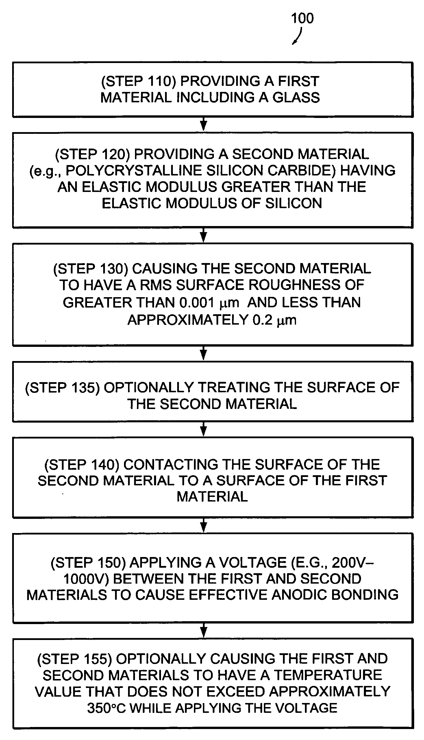
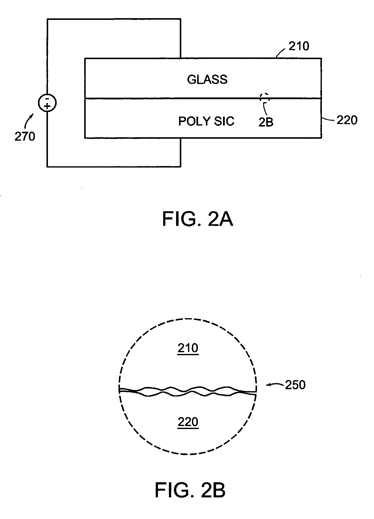
[0025]FIG. 1 is a flowchart of a method 100 for anodic bonding according to an illustrative embodiment of the invention. The method 100 includes providing a first material including a glass (Step 110), providing a second material having an elastic modulus greater than the elastic modulus of silicon (Step 120), causing the second material to have a RMS surface roughness of greater than 0.001 μm and, preferably, less than approximately 0.15 μm (Step 130), contacting the surface of the second material to a surface of the first material (Step 140), and applying a voltage between the first and second materials to cause effective anodic bonding (Step 150). An effective anodic bond is one that attaches the first material to the second material with satisfactory reliability under handling and use conditions.
[0026] Before bonding, the surface of the second material may be treated (Step 135). For example, a hydrophobic surface treatment may be applied to the surface. An effective bond may be...
PUM
| Property | Measurement | Unit |
|---|---|---|
| RMS surface roughness | aaaaa | aaaaa |
| RMS surface roughness | aaaaa | aaaaa |
| temperature | aaaaa | aaaaa |
Abstract
Description
Claims
Application Information