"Low power silicon thermal sensors and microfluidic devices based on the use of porous sealed air cavity technology or microchannel technology"

Inactive Publication Date: 2005-04-07
NASSIOPOULOU ANDROULA G +2
View PDF8 Cites 12 Cited by
  • Summary
  • Abstract
  • Description
  • Claims
  • Application Information

AI Technical Summary

Benefits of technology

[0003] It is an object of this invention to provide a method for the fabrication of silicon thermal sensors with improved thermal isolation, based on the use of a sealed cavity on which the active elements of the sensor are developed. The sealed cavity is fabricated on bulk silicon by a two-step electrochemical process in which in the first step porous silicon is formed locally on bulk silicon by electrochemical dissolution with an anodization current below the limit for electropolishing and in a second step the current is increased so as the process is turned to electropolishing for the fabrication of a cavity underneath the porous layer. The silicon thermal sensor devices based on the above structure combine the good isolation properties offered by suspended membranes with the advantage of having a rigid structure. In the Greek patent No. OBI 1003010, a rigid and mechanically stable structure was also propose

Problems solved by technology

However, there is an important drawback in the above techniques.
It is related to the fragi

Method used


Image

  • "Low power silicon thermal sensors and microfluidic devices based on the use of porous sealed air cavity technology or microchannel technology"
  • "Low power silicon thermal sensors and microfluidic devices based on the use of porous sealed air cavity technology or microchannel technology"
  • "Low power silicon thermal sensors and microfluidic devices based on the use of porous sealed air cavity technology or microchannel technology"

Examples


Example

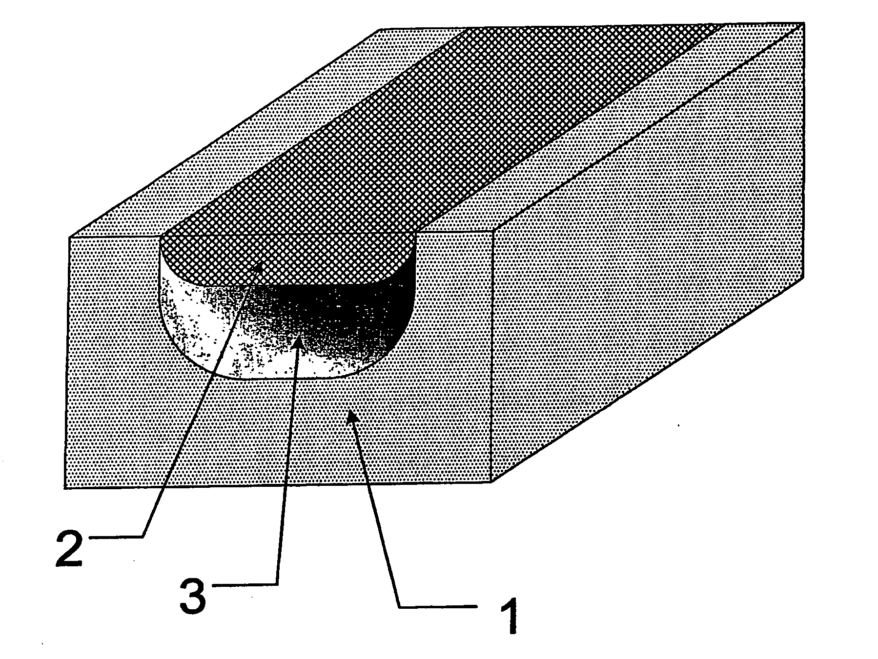
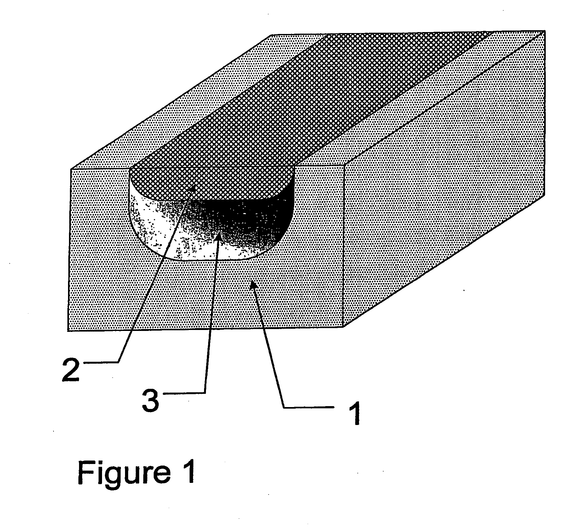
[0018]FIG. 1 is a schematic representation of a silicon substrate (1) with a porous silicon layer (2) on top of a cavity (3). The whole structure is used for local thermal isolation on bulk silicon.

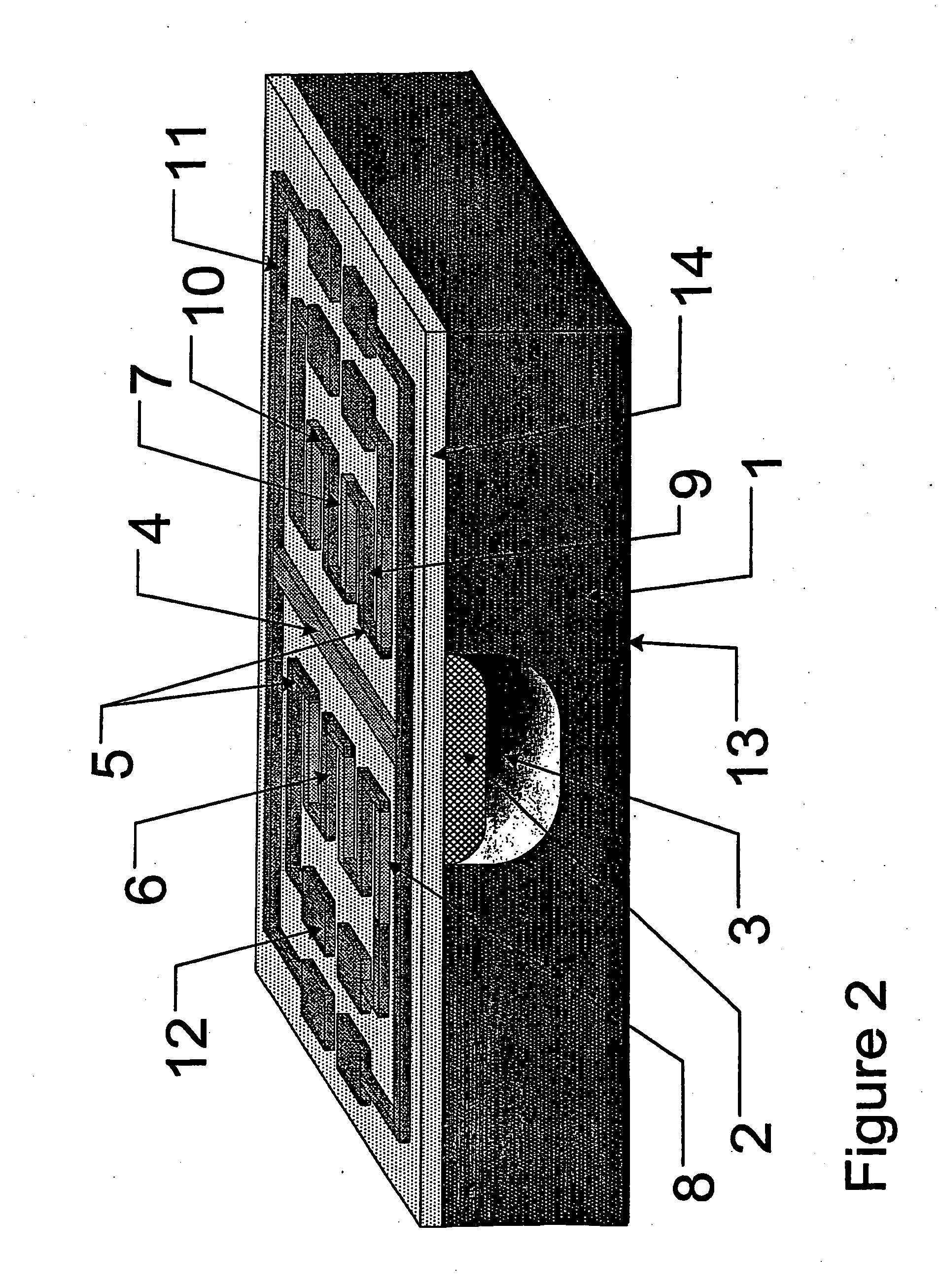
[0019]FIG. 2 is a schematic representation of a silicon thermal gas flow sensor. The base material is p-type silicon (1) in which a porous silicon membrane (2) with a cavity (3) underneath is formed.

[0020] On top of the porous silicon cavity area a polysilicon resistor (4) is formed and two series of thermocouples are integrated on each side of this resistor (6, 7). The hot contacts (5) of these thermopiles lie on porous silicon and the cold contacts (10) on bulk crystalline silicon. There are also aluminum pads (12) used as electrical contacts.

[0021]FIG. 3 shows the temperature on heater for thermal isolation by porous silicon of variable thickness over a cavity for a power of 8.57×10⁶ W / m2 applied on the heater.

[0022]FIG. 4 shows the temperature on heater for thermal isolation by a ...


PUM

PropertyMeasurementUnit
Temperatureaaaaaaaaaa
Flow rateaaaaaaaaaa
Currentaaaaaaaaaa

Abstract

This invention provides a miniaturized silicon thermal flow sensor with improved characteristics, based on the use of two series of integrated thermocouples (6, 7) on each side of a heater (4), all integrated on a porous silicon membrane (2) on top of a cavity (3). Porous silicon (2) with the cavity (3) underneath provides very good thermal isolation for the sensor elements, so as the power needed to maintain the heater (4) at a given temperature is very low. The formation process of the porous silicon membrane (2) with the cavity (3) underneath is a two-step single electrochemical process. It is based on the fact that when the anodic current is relatively low, we are in a regime of porous silicon formation, while if this current exceeds a certain value we turn into a regime of electropolishing. The process starts at low current to form porous silicon (2) and it is then turned into electropolishing conditions to form the cavity (3) underneath. Various types of thermal sensor devices, such as flow sensors, gas sensors, IR detectors, humidity sensors and thermoelectric power generators are described using the proposed methodology. Furthermore the present invention provides a method for the formation of microfluidic channels (16) using the same technique of porous silicon (17) and cavity (16) formation.

Description

FIELD OF THE INVENTION [0001] This invention relates to low power silicon thermal sensors and microfluidic devices, which use a micromachining technique to fabricate electrochemically porous silicon membranes with a cavity underneath. In the case of thermal sensors the structure used is of the closed type (porous silicon membrane on top of a cavity), while in microfluidics the same technique is used to open microchannels with a porous silicon membrane on top. DESCRIPTION OF THE RELATED ART [0002] Silicon thermal flow sensors are based on heat exchange between the fluid and the hot parts of the device, which are kept at relatively high temperature, of the order of 100-180° C. In silicon thermal gas sensors, this temperature has, sometimes, to exceed 400° C. In order to keep the temperature constant, the electric power on the heater has to compensate thermal losses due to conduction, convection and radiation. Losses due to conduction through the substrate on which the active elements ...

Claims


Application Information

Patent Timeline
IPC IPC(8): G01K13/02B81B1/00B81B3/00B81C1/00G01F1/684G01K7/01G01K7/02
CPCB81B2201/058B81B2203/0127B81B2203/0315G01K7/028B81C2201/0114B81C2201/0115G01F1/6845B81C1/00071
Inventor NASSIOPOULOU, ANDROULA G.KALTSAS, GRIGORISPAGONIS, DIMITRIOS N.
Owner NASSIOPOULOU ANDROULA G
Why Eureka
Try Eureka