Switched-capacitor sample/hold having reduced amplifier slew-rate and settling time requirements

Active Publication Date: 2005-04-07
MICROCHIP TECH INC
View PDF6 Cites 27 Cited by
  • Summary
  • Abstract
  • Description
  • Claims
  • Application Information

AI Technical Summary

Benefits of technology

[0010] The above objective of providing a switched-capacitor sample/hold circuit having a reduced amplifier slew rate and settling time requirement and reduced error due to amplifier slew rate and settling time is provided in a new switched-capacitor sample/hold circuit and method of operation of a sample/hold circuit. The above objectives of reducing error due to charge injection and improving linearity is provided in a differential embodiment of the circuit and method of the present invention.
[0011] The new switched-capacitor sample/hold circuit includes two capacitors, both of which are alternatively and mutually-exclusively placed in an input sampling position and an amplifier feedback hold position, providing a double sampling of the input signal that reduces the magnitude of transitions on the output of the sample/hold amplifier.
[0012

Problems solved by technology

The slew rate and setting time of the amplifier are a source of error in the switched-capacitor sample/hold circuit.
The slew rate and settling time are cost drivers for the amplifier, and within an integrated circuit can mean increased area and power dissipation and/or increased voltage requirements.
Another source of error in switched-capacitor circuits in general, and switched-capacitor sample/hold circuits in particular, is erro

Method used


Image

  • Switched-capacitor sample/hold having reduced amplifier slew-rate and settling time requirements
  • Switched-capacitor sample/hold having reduced amplifier slew-rate and settling time requirements
  • Switched-capacitor sample/hold having reduced amplifier slew-rate and settling time requirements

Examples


Embodiment Construction

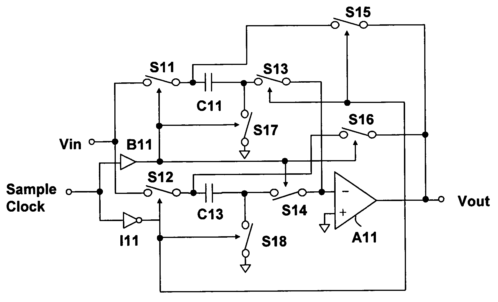
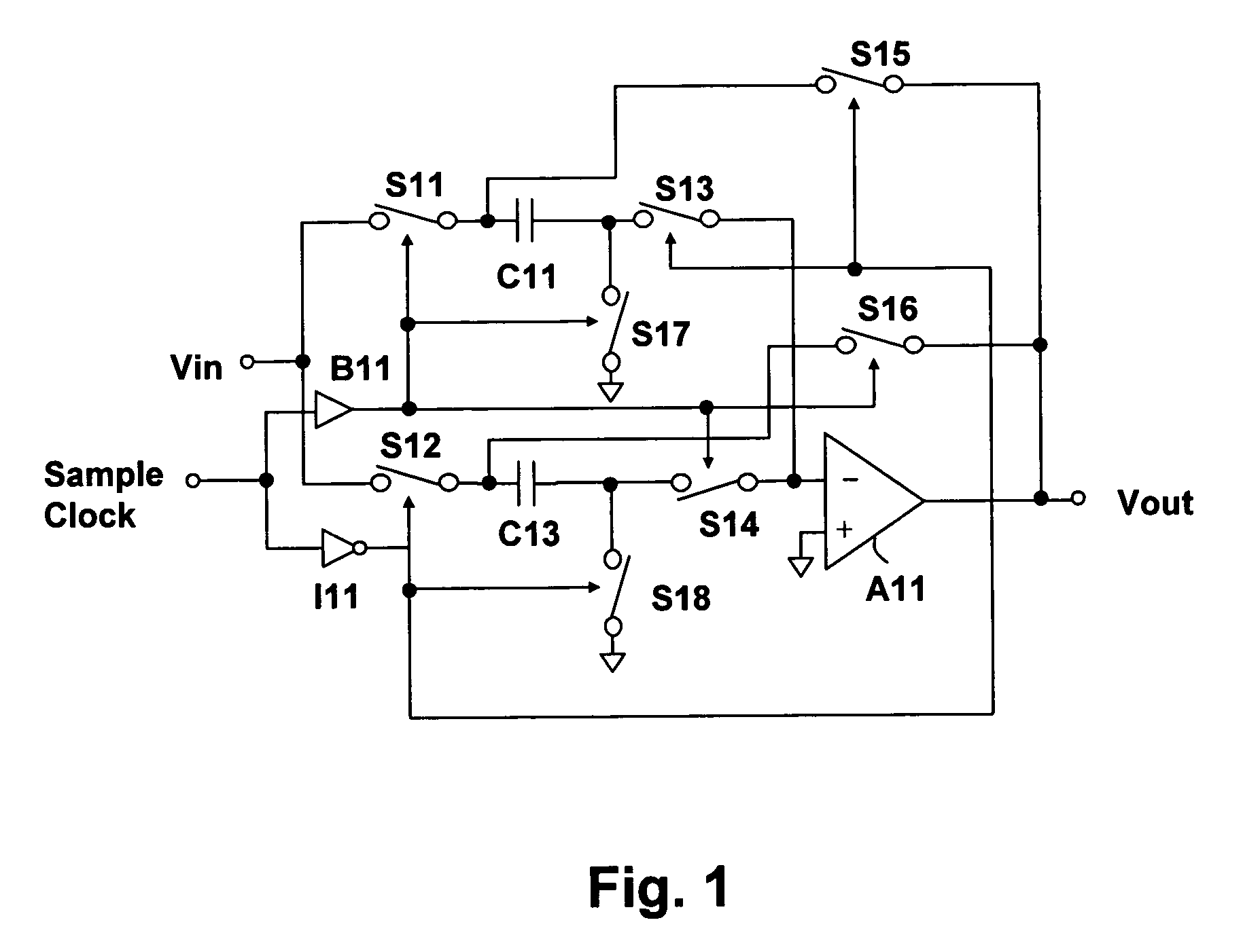
[0021] Referring now to the figures, and in particular to FIG. 1, a sample / hold circuit in accordance with an embodiment of the invention is depicted. An input voltage Vin is alternatively applied to a first capacitor C11 or a second capacitor C13 via switches S11 and S12 to sample an input signal. When capacitor C11 is selected for sampling, switch S17 is closed, grounding a second terminal of capacitor C11, similarly switch S18 grounds a second terminal of capacitor C13, when capacitor C13 is selected for sampling. The capacitor (C11 or C13) that is not selected for sampling is connected via switches S13 and S15 (for C11) or switches S14 and S16 (for C13) in the feedback path of an amplifier A11, which provides a sampled output Vout. The control signals for switches S11-S18 are provided by buffer B11 and inverter I11 so that two complementary phases of the sampling clock signal are provided for selecting the alternate states required for switches S11-S18. The circuit of FIG. 1 is ...


PUM


Abstract

A switched-capacitor sample/hold circuit and method having reduced slew-rate and settling time requirements provides for lower-cost and/or lower-power implementation of sample/hold circuits and/or reduced error due to amplifier characteristics. The switched-capacitor sample/hold circuit incorporates a pair of capacitors that are alternatively and mutually-exclusively switched between an input sample position and an amplifier hold position, providing a dual sampled amplifier output signal that has reduced transitions at each sample interval. An alternative embodiment of the sample/hold circuit incorporates a fully-differential amplifier having a differential input and a differential output. Four capacitors are employed forming two of the dual sampled switched-capacitor circuits, one in each negative feedback path (inverted output to non-inverting input, non-inverted output to inverting input) of the amplifier. The two dual sampled switched-capacitor circuits are referenced to each other, providing fully differential operation and cancellation of error due to charge injection.

Description

BACKGROUND OF THE INVENTION [0001] 1. Field of the Invention [0002] The present invention relates generally to analog signal sampling circuits, and more specifically, to a switched-capacitor sample / hold having reduced amplifier slew-rate and settling time requirements. [0003] 2. Background of the Invention [0004] Switched-capacitor sample / hold circuits are in common use today. Integrated circuits such as analog-to-digital (A / D) converters as well as voltage-to-frequency (V / F) converters, switched capacitor filters and other analog signal processing components often incorporate switched-capacitor circuits and in particular switched-capacitor sample / hold circuits to provide sampling and filtering circuits with controllable gain and circuit performance. [0005] The simplest form of sample / hold circuit utilizes a single capacitor and a switch that samples the input signal onto the capacitor for a fixed interval. The capacitor is followed by a buffer amplifier that isolates subsequent sta...

Claims


Application Information

Patent Timeline
IPC IPC(8): G06G7/18H03F3/00H03F3/45
CPCH03F3/45475H03F3/005
Inventor KO, TERASUTHWONG, CHI CHUN
Owner MICROCHIP TECH INC
Why Eureka
Try Eureka