

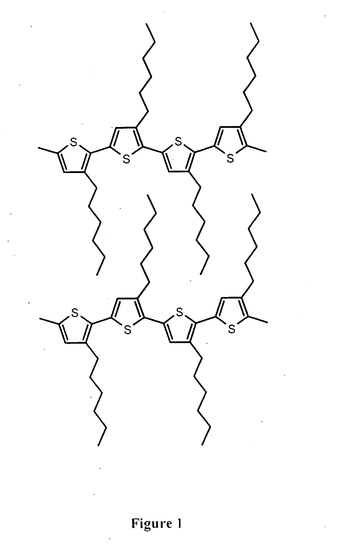
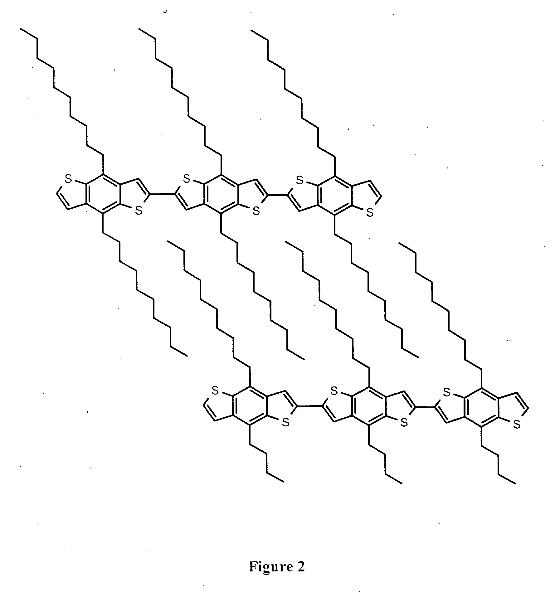
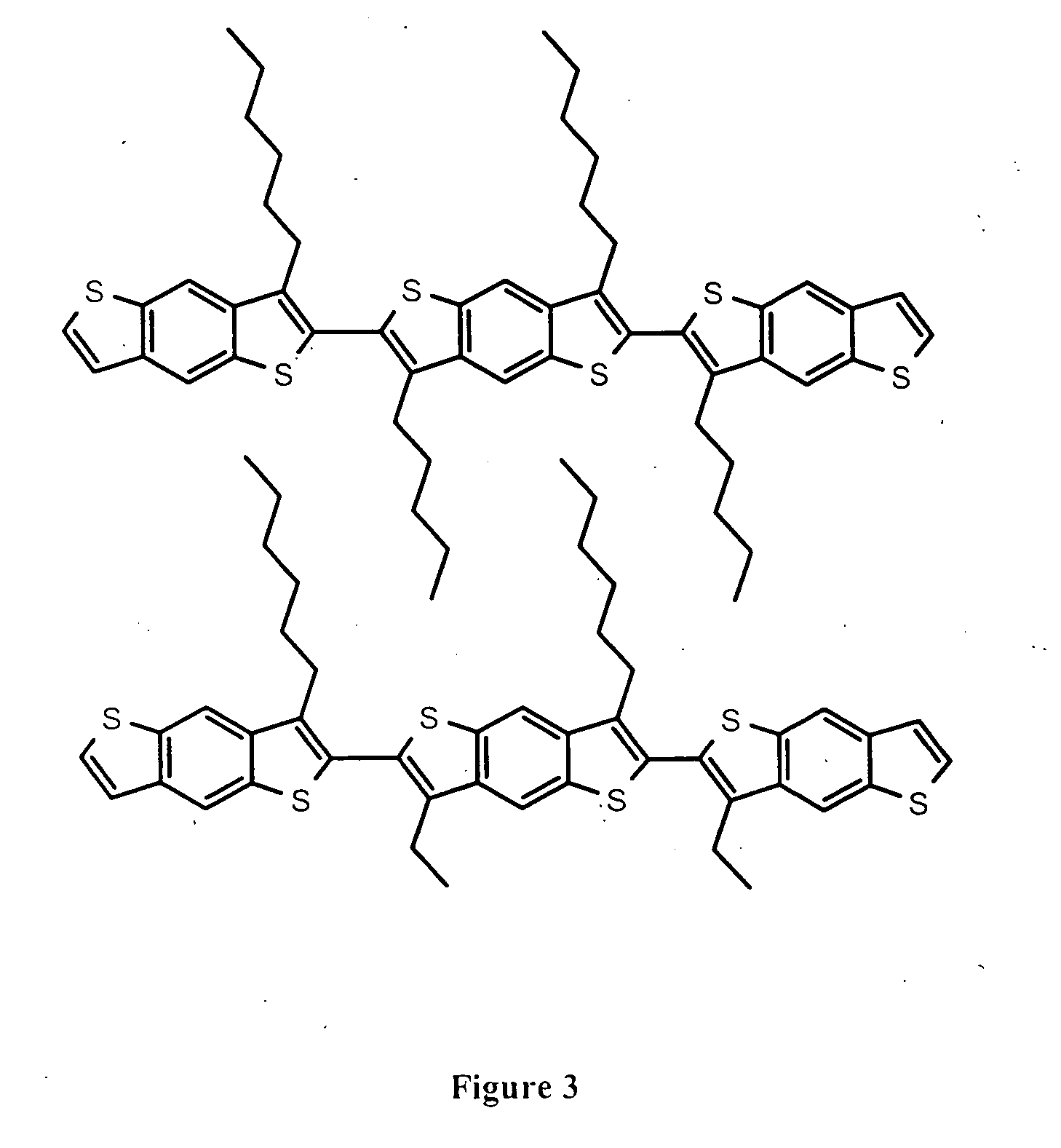
Poly(benzodithiophenes)
a technology of benzodithiophene and poly(3-alkylthiophene) is applied in the field of poly(benzodithiophene), which can solve the problems of reducing device performance, oxidative instability of materials, and low ionization potential of poly(3-alkylthiophene),
- Summary
- Abstract
- Description
- Claims
- Application Information
AI Technical Summary
Benefits of technology
Problems solved by technology
Method used
Image

Examples
example 1
[0120] Poly-(4,8-dihexylbenzo[1,2-b;4,5-b′]dithiophene) (1d) is prepared as shown in Scheme 1 above.
1a) Sodium [1,3]dioxolan-2-ylmethanethiolate
[0121] 2-Bromomethyl[1,3]dioxolane (101.2 g, 0.606 mol) and potassium thioacetate (70.8 g, 0.620 mol) in DMF (700 mL) are stirred at 40° C. for 70 h under nitrogen. The reaction mixture is cooled to RT and filtered. The solvent is removed under reduced pressure. The residue is dissolved in DCM (400 mL) and washed with water (400 mL). The aqueous layer is extracted again with DCM (2×1 00 mL). The combined extracts are washed with brine (2×100 mL), dried over sodium sulfate, and concentrated in vacuo. The residue is filtered through silica (eluent: DCM) and concentrated in vacuo to afford_thioacetic acid S-[1,3]dioxolan-2-ylmethyl ester (97.1 g, 99%). Thioacetic acid S-[1,3]dioxolan-2-ylmethyl ester (63.4 g, 0.391 mol) and sodium methoxide (21.6 g, 0.400 mol) in anhydrous methanol (1 L) are stirred at RT for 12 h. The solvent is removed und...
example 2
[0125] Poly-(4,8-didecylbenzo[1,2-b;4,5-b′]dithiophene) (2d) is prepared as shown in Scheme 1 above.
2a) 2.5-Dibromo-, 4-didecylbenzene
[0126] 2,5-Dibromo-1,4-didecylbenzene is prepared from 1,4-dibromobenzene in two steps according to literature procedures: decylmagnesium bromide is coupled to 1,4 dibromobenzene using PdCl2(dppf) to yield 1,4-didecylbenzene, which is subsequently treated with bromine to afford 2,5-dibromo-1,4-didecylbenzene.
2b) 2,5-Bis([ ]. 3dioxolan-2-ylmethanethiolato)-1,4-didecylbenzene
[0127] A 3-necked flask is charged with sodium [1,3]dioxolan-2-ylmethanethiolate (2.84 g, 20.00 mmol) and sodium tert-butoxide (2.31 g, 20.00 mmol) and purged with nitrogen. Anhydrous toluene (50 mL) is added and the reaction mixture is stirred at RT overnight. Palladium(II) acetate (0.18 g, 0.80 mmol), rac-BINAP (0.55 g, 0.88 mmol) and 2,5-dibromo-1,4-didecylbenzene (4.13 g, 8.00 mmol) are added and the reaction mixture is stirred at 80° C. for 48 h. The reaction mixture is co...
PUM
| Property | Measurement | Unit |
|---|---|---|
| melting point | aaaaa | aaaaa |
| charge transport properties | aaaaa | aaaaa |
| charge transport | aaaaa | aaaaa |
Abstract
Description
Claims
Application Information