Method for preapplying a viscous material to strengthen solder connections in microelectronic packaging and microelectronic packages formed thereby

a technology of viscous material and microelectronic packaging, applied in the field of microelectronic packaging, can solve the problems of short life, short circuit, short circuit, etc., and achieve the effect of improving the workability of an underfilled component, simple removal, and cost reduction

Inactive Publication Date: 2005-04-21
NORDSON CORP
View PDF12 Cites 28 Cited by
  • Summary
  • Abstract
  • Description
  • Claims
  • Application Information

AI Technical Summary

Benefits of technology

[0011] In accordance with principles of the invention, the reworkability of an underfilled component is improved without sacrificing, or otherwise compromising, the ability of the underfill material to provide solder joint reliability. The underfill material wets up the side of each solder bump. This wetting may produce a concave profile. In addition, a thin layer of underfill material may be present in the interstices or spaces between adjacent bumps. The thin layer may be continuous. However, the underfill material does not bridge the gap between the packaging substrate and component (i.e., does not contact the underside of the packaging substrate). Therefore, the underfill material does not have to be removed during rework and the component can be simply removed by heating and reflowing the solder joints. After removal, the solder bumps

Problems solved by technology

The presence of the cured underfill material also discourages dendrite growth and other moisture-based failure mechanisms potentially causing electrical shorting and component failure.
Although the cured underfill material improves package reliability, it hinders component removability and the important rework option.
However, in such no-flow processes, the preapplied underfill material should not contaminate the crown of the solder bumps as the electrical connections may never be effectively esta

Method used


Image

  • Method for preapplying a viscous material to strengthen solder connections in microelectronic packaging and microelectronic packages formed thereby
  • Method for preapplying a viscous material to strengthen solder connections in microelectronic packaging and microelectronic packages formed thereby
  • Method for preapplying a viscous material to strengthen solder connections in microelectronic packaging and microelectronic packages formed thereby

Examples


Embodiment Construction

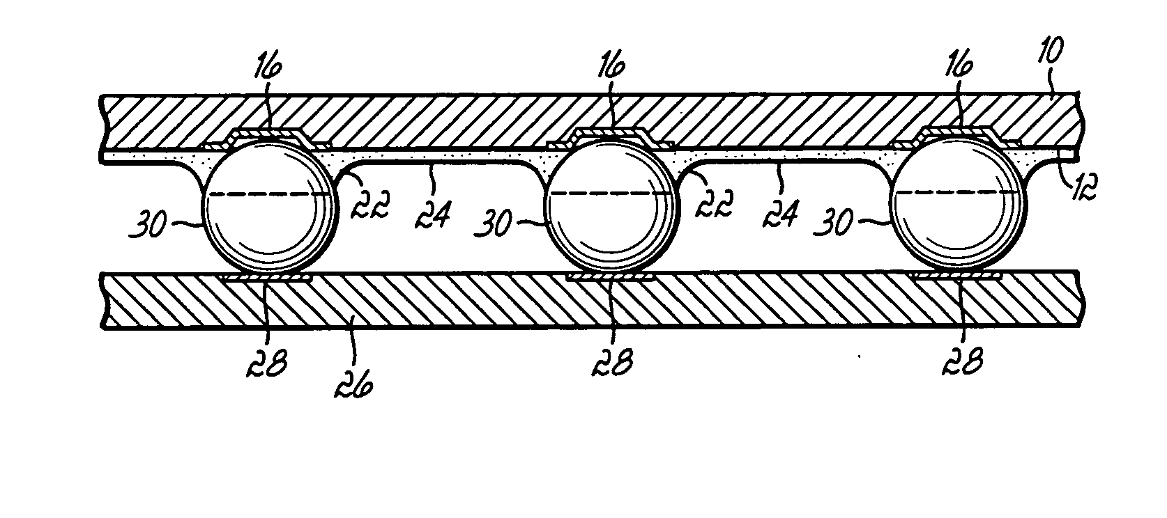
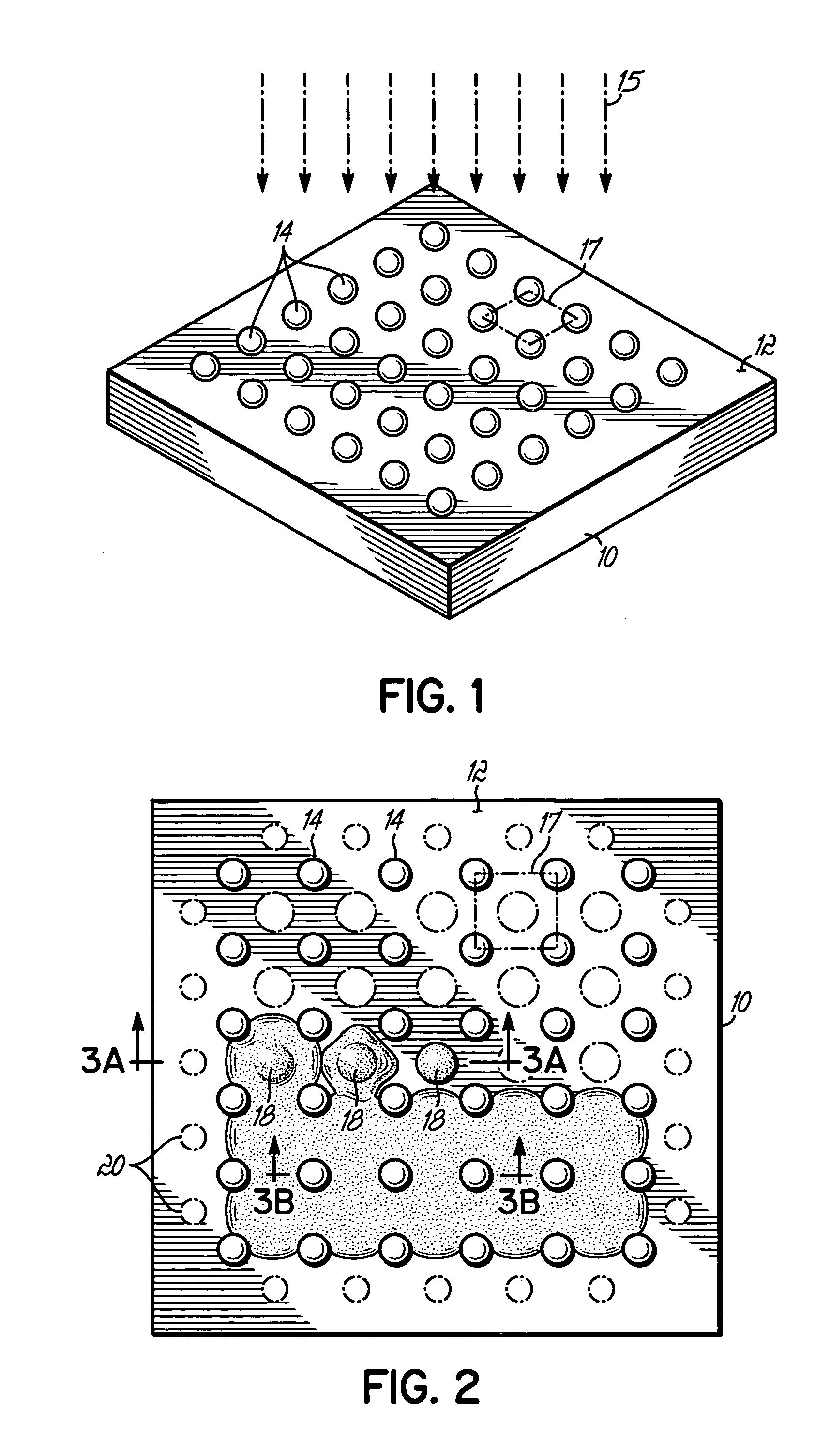
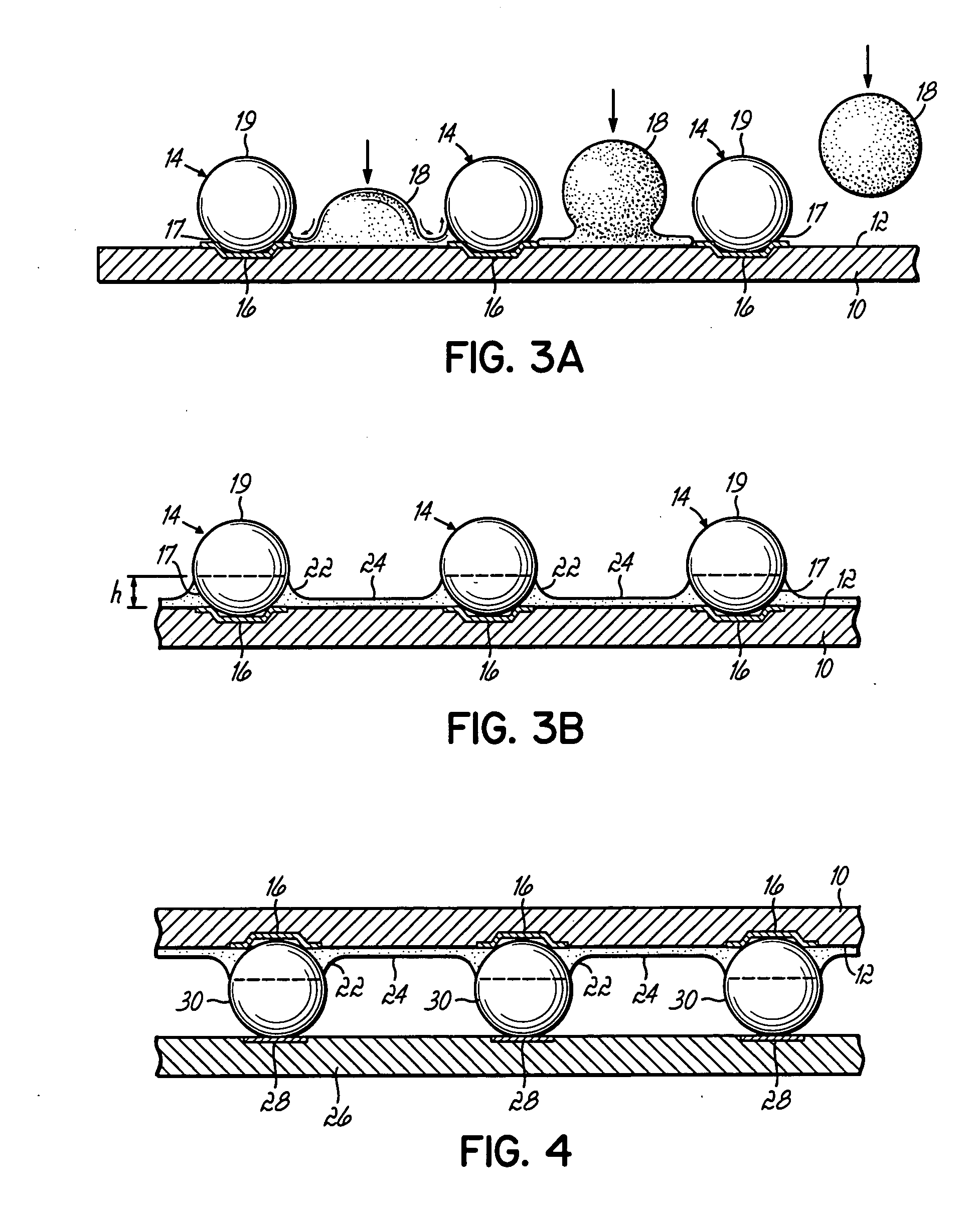
[0020] With reference to FIG. 1, a component 10, such as a semiconductor die or chip, includes a substrate 12 with an active surface that carries a plurality of solder balls or bumps 14 arranged in a matrix or an array, such as a ball grid array or a pin grid array. Typically, the array of solder bumps 14 is symmetrical and each bump 14 is hemispherical, although the invention is not so limited. The solder bumps 14 may be solder bodies of any conventional shape or construction description known by persons of ordinary skill in the art that join one surface to another leaving an air gap between the joined surfaces. The solder constituting the solder bumps 14 may be composed, for example, of a low melting point eutectic material or a high lead material. The solder bumps 14 may be formed or placed on the UBM-covered bond pads 16 by any suitable process, including but not limited to evaporation, electroplating, printing, jetting, stud bumping, and direct placement.

[0021] Before the unde...


PUM


Abstract

Apparatus and methods for preapplying discrete amounts of underfill material of a component on a component substrate before the solder bumps of the component are joined by reflow with a packaging substrate to create a microelectronics package. The underfill material is preferably applied by a noncontact dispensing technique as discrete amounts at interstitial areas on an active surface of the component substrate defined between nearest-neighbor solder bumps. The underfill material forms a continuous meniscus of underfill material across the interstitial areas not occupied by the solder bumps and forms a collar encircling each of the solder bumps. The cured underfill material strengthens and improves the reliability of the solder joints formed by the bump reflow.

Description

FIELD OF THE INVENTION [0001] This invention relates generally to microelectronic packaging and, more particularly, to preapplying a viscous material to solder bumps on a component before the solder bumps are reflowed to form a microelectronic package with a packaging substrate and microelectronic packages formed thereby. BACKGROUND OF THE INVENTION [0002] In microelectronic packaging, components, such as semiconductor die or chips, are mounted on a packaging substrate, such as a printed circuit board or a leadframe. Typically, solder balls or bumps on the component are placed in registration with electrical bond pads or electrical traces on the packaging substrate and the solder bumps are then reflowed to create electrical and mechanical interconnections in the form of solder joints extending between the component and the packaging substrate. After the reflow process is complete, a space or gap is present between the component and the packaging substrate. [0003] Filling the gap wit...

Claims


Application Information

Patent Timeline
IPC IPC(8): H01L21/56H01L23/31
CPCH01L21/563H01L23/3114H01L23/3171H01L2924/01322H01L2224/73203H01L2924/0102H01L24/10H01L2224/05572H01L2224/05573H01L2224/13022
Inventor QUINONES, HORATIOFANG, LIANGELLIS, DAVEFISKE, ERIK ANDREWRATLEDGE, THOMAS LAFERLBABIARZ, ALEC J.CIARDELLA, ROBERT
Owner NORDSON CORP
Why Eureka
Try Eureka