Silicon chip carrier with through-vias using laser assisted chemical vapor deposition of conductor

a silicon chip carrier and through-via technology, applied in the field of integrated circuits, can solve the problems of inability to achieve electroplating or electroless processes for w, mo, or ta, and the common method of via filling of integrated circuit interconnects become technically problematic or impractical, and achieve the effect of high aspect ratio

Active Publication Date: 2005-04-21
ELPIS TECH INC
View PDF3 Cites 85 Cited by
  • Summary
  • Abstract
  • Description
  • Claims
  • Application Information

AI Technical Summary

Benefits of technology

[0014] An aspect of the present invention provides a high aspect ratio via having a depth of from about 100 to 300 micrometers and an aspect ratio of from about 3:1 to about 10:1.

Problems solved by technology

Via fill methods common to integrated circuit interconnects become technically problematic or impractical when trying to fill such large blind holes (to be opened later).
However, paste-filled vias are associated with an undesirably high degree of porosity.
However, no electroplating or electroless processes presently exist for W, Mo, or Ta.
Plasma jet processes are unsuitable for filling high aspect ratio vias because their high deposition rates, result in porous metal structures.
Such heating of the SiO2 would lead to metal deposition at undesired locations.
Because the laser must couple with the substrate in order to deposit metal thereon, the substrate is limited to materials such as Si.
Therefore, prior art processes do not permit tungsten to be deposited directly on SiO2, but are limited to deposition on Si or metal.
An additional drawback of prior art processes is that SiO2 thicknesses and via dimensions are altered due to HF etching.

Method used


Image

  • Silicon chip carrier with through-vias using laser assisted chemical vapor deposition of conductor
  • Silicon chip carrier with through-vias using laser assisted chemical vapor deposition of conductor
  • Silicon chip carrier with through-vias using laser assisted chemical vapor deposition of conductor

Examples


Embodiment Construction

[0045] Reference is made to the figures to illustrate selected embodiments and preferred modes of carrying out the invention. It is to be understood that the invention is not hereby limited to those aspects depicted in the figures.

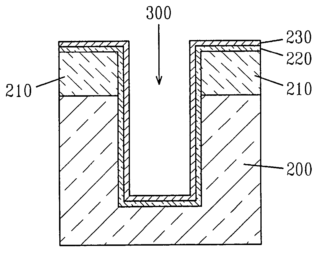
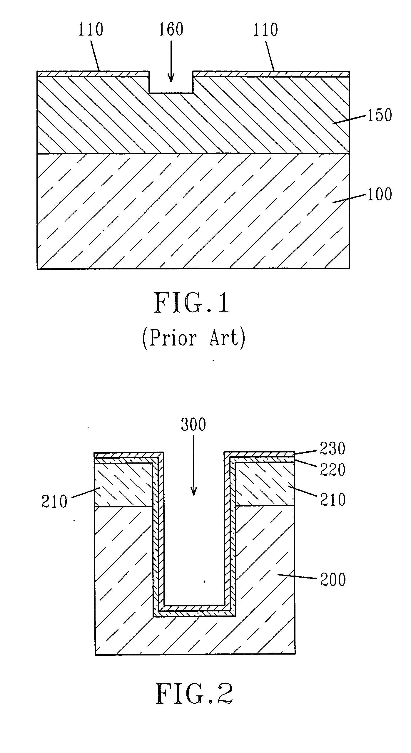
[0046] This invention is directed to insulated, conductive through-vias formed in a self-supporting carrier substrate. The requirement that the substrate be self-supporting implies a thickness of from about 100 to 700 micrometers. The inventive vias are initially formed as blind-vias. However, it is intended that they be opened to form through-vias. For purposes of the present invention, via cavities may be formed by any of a variety of methods known to the art.

[0047] Fabrication process practicalities place lower limits on via diameters. Given realistic substrate thicknesses of up to 700 micrometers and realistic via aspect ratios (e.g. 3:1 to 10:1), via diameters must range from about 10 micrometers to greater than 200 micrometers. Via fill methods com...


PUM

PropertyMeasurementUnit
thicknessaaaaaaaaaa
thicknessaaaaaaaaaa
thicknessaaaaaaaaaa

Abstract

This disclosure teaches a method of filling deep vias or capping deep conducting paste filled vias in silicon or glass substrate using laser assisted chemical vapor deposition of metals. This method uses a continuous wave or pulsed laser to heat the via bottom and the growing metal fill selectively by selecting the laser wavelength such that silicon and/or glass do not absorb the energy of the laser in any appreciable manner to cause deposition in the field. Alternatively holographic mask or an array of micro lenses may be used to focus the laser beams to the vias to fill them with metal. The substrate is moved in a controlled manner in the z-direction away from the laser at about the rate of deposition thus causing the laser heating to be focused on the surface region of the growing metal fill.

Description

FIELD OF THE INVENTION [0001] The present invention relates generally to integrated circuits, and particularly, but not by way of limitation, to a semiconductor or glass substrate-based carrier for mounting and packaging multiple integrated circuit chips and / or other devices. The carrier is a freestanding chip or wafer with insulated, conductive through-vias exposed on top and underside, to connect flip-chip and other device I / O through the carrier to next-level package, board, or other flip-chips mounted on the bottom side. The present invention relates to filling a blind-via with a metal rod. Subsequent to forming a metal-filled, blind via, and subsequent to any optional frontside processing the invention contemplates the opening of the bottom of the via thereby forming a through-via. Opening a via from the backside is taught in U.S. Pat. No. 6,593,644 and in co-pending application (number not yet assigned, Attorney Docket Number YOR9-2003-0098-US1). These references are assigned ...

Claims


Application Information

Patent Timeline
Patent Type & Authority Applications(United States)
IPC IPC(8): H01L21/768H01L23/48
CPCH01L21/76898H01L23/481H01L2924/0002H01L2924/00
Inventor ANDRY, PAUL STEPHENBUCHWALTER, LEENA PAIVIKKIBUDD, RUSSELL ALANWASSICK, THOMAS ANTHONY
Owner ELPIS TECH INC
Why Eureka
Try Eureka