Structure and method to enhance both nFET and pFET performance using different kinds of stressed layers

a technology of stress layer and nfet, which is applied in the direction of semiconductor/solid-state device details, electrical apparatus, semiconductor devices, etc., can solve the problems of signal propagation time and susceptibility, the length of propagation path, and the cost of devices containing chips, so as to enhance both nfet and pfet performance

Inactive Publication Date: 2005-05-05
GLOBALFOUNDRIES INC
View PDF17 Cites 200 Cited by
  • Summary
  • Abstract
  • Description
  • Claims
  • Application Information

AI Technical Summary

Benefits of technology

[0009] It is therefore an object of the present invention to provide a structure and method to enhance both nFET and pFET performance by

Problems solved by technology

That is, increased integration density and proximity of elements reduces the signal propagation path length and reduces signal propagation time and susceptibility to noise and increase of possible clock rates while the reduction in element size necessary for increased integration density increases the ratio of functionality which can be provided on a chip to the costs of production (e.g. wafer/chip area and process materials) per chip and, potentially, the cost of devices containing the chips by reducing the number of inter-chip and inter-board connections required.
However, the immutable material properties and physical effects by which transistors and other elements function is invariably compromised as the scale of integrated circuit elements is reduced.
In more recent and critical designs, it has been shown that carrier mobility degrades in deeply scaled bulk MOS devic

Method used


Image

  • Structure and method to enhance both nFET and pFET performance using different kinds of stressed layers
  • Structure and method to enhance both nFET and pFET performance using different kinds of stressed layers
  • Structure and method to enhance both nFET and pFET performance using different kinds of stressed layers

Examples


Embodiment Construction

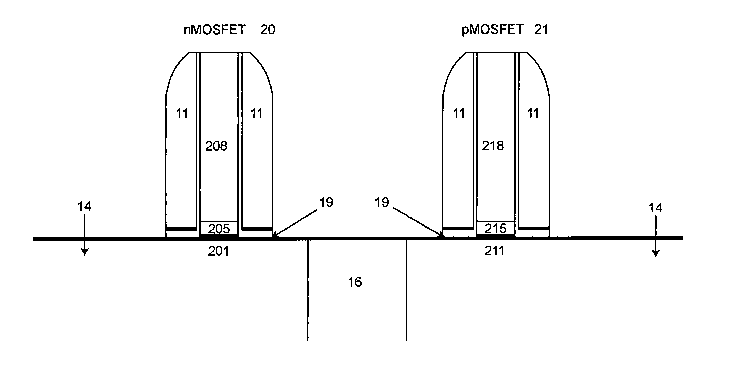
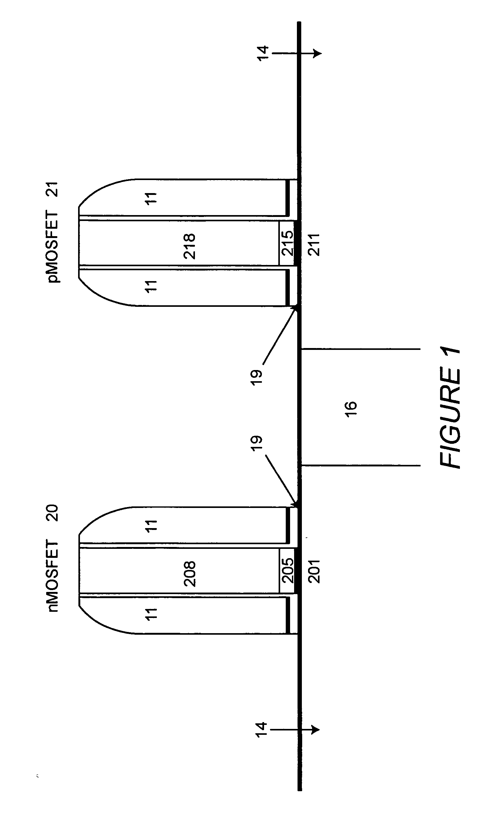
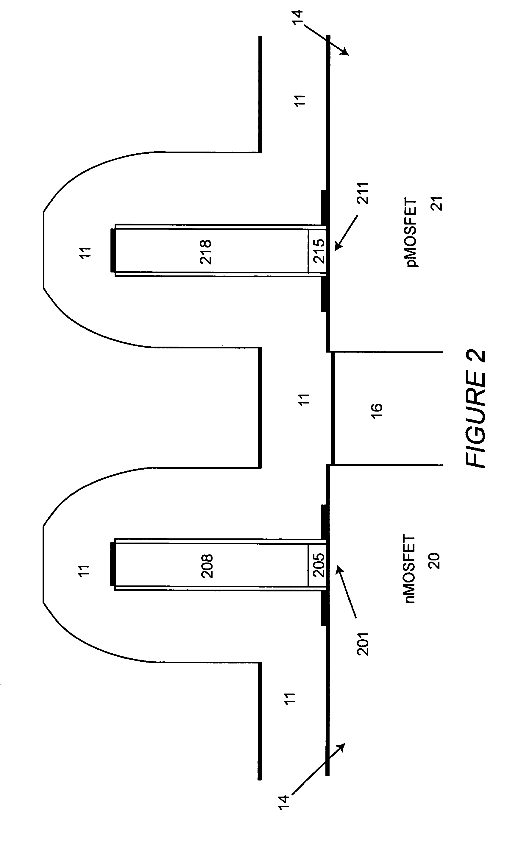
[0024] Referring now to the drawings, and more particularly to FIG. 1, there is shown, in cross-section, an exemplary pair of complementary nMOS and pMOS transistors such as might comprise a CMOS pair in a portion of an integrated circuit. These transistors have been completed through the formation of silicide on the source, drain and gate regions to reduce resistance of contacts to be later applied thereto. The method of formation of these transistors and the particulars of their structures are unimportant to an understanding of the invention or its successful practice. It should be understood that while FIG. 1 illustrates transistors prior to the application of the invention thereto, the illustration is intended to be highly schematic for clarity and no portion of FIG. 1 is admitted to be prior art as to the invention.

[0025] In FIG. 1 and other figures, the transistors are formed on substrate 14 (which may be relatively much thicker than depicted since the transistors are possibl...


PUM


Abstract

In producing complementary sets of metal-oxide-semiconductor (CMOS) field effect transistors, including nMOS and pMOS transistors), carrier mobility is enhanced or otherwise regulated through the use of layering various stressed films over either the nMOS or pMOS transistor (or both), depending on the properties of the layer and isolating stressed layers from each other and other structures with an additional layer in a selected location. Thus both types of transistors on a single chip or substrate can achieve an enhanced carrier mobility, thereby improving the performance of CMOS devices and integrated circuits.

Description

BACKGROUND OF THE INVENTION [0001] 1. Field of the Invention [0002] The present invention generally relates to the manufacture of transistors for integrated circuits and, more particularly, to the production of complementary pairs of field effect transistors of enhanced performance at extremely small scale. [0003] 2. Description of the Prior Art [0004] Performance and economic factors of integrated circuit design and manufacture have caused the scale of elements (e.g. transistors, capacitors and the like) of integrated circuits to be drastically reduced in size and increased in proximity on a chip. That is, increased integration density and proximity of elements reduces the signal propagation path length and reduces signal propagation time and susceptibility to noise and increase of possible clock rates while the reduction in element size necessary for increased integration density increases the ratio of functionality which can be provided on a chip to the costs of production (e.g. ...

Claims


Application Information

Patent Timeline
IPC IPC(8): H01L21/8238
CPCH01L21/823807H01L21/823828H01L29/7843H01L29/6653H01L29/7842H01L21/823864
Inventor DORIS, BRUCE B.YANG, HAININGZHU, HUILONG
Owner GLOBALFOUNDRIES INC
Why Eureka
Try Eureka