Semiconductor integrated circuit device

a technology of integrated circuits and semiconductors, applied in semiconductor devices, semiconductor/solid-state device details, electrical apparatus, etc., can solve problems such as affecting the high-speed operation of devices, and achieve the effects of suppressing electromigration and stress migration, high-speed operation of devices, and extending wiring li

Inactive Publication Date: 2005-05-05
RENESAS ELECTRONICS CORP
View PDF18 Cites 7 Cited by
  • Summary
  • Abstract
  • Description
  • Claims
  • Application Information

AI Technical Summary

Benefits of technology

[0015] It is accordingly an object of the invention to provide a semiconductor integrated circuit device and a method of manufacture thereof wherein a cap conductive film is formed on a wiring, thereby realizing high speed operation of the device.
[0016] It is another object of the invention to provide a semiconductor integrated circuit device and a method of manufacture thereof wherein an elongated wiring life is ensured, while suppressing electromigration and stress migration from occurring.
[0017] It is a further object of the invention to provide a semiconductor integrated circuit device and a method of manufacture thereof wherein the device has an improved dielectric breakdown and has a reduced leakage current achieved by preventing direct sputtering of an underlying copper wiring when a contact hole is etched at the bottom thereof.
[0018] It is a still further object of the invention to provide a semiconductor integrated circuit device and a method of manufacture thereof wherein contact failure is reduced even if a contact hole is shifted relative to a wiring.

Problems solved by technology

Since the silicon nitride film has a high dielectric constant, the RC time constant of the wiring becomes great, thereby impeding the high-speed operation of the device.

Method used


Image

  • Semiconductor integrated circuit device
  • Semiconductor integrated circuit device
  • Semiconductor integrated circuit device

Examples


embodiment 1

[0062]FIGS. 1a to 11 are, respectively, sectional views showing the successive steps of a method of manufacture of a semiconductor integrated circuit device according to Embodiment 1 of the invention.

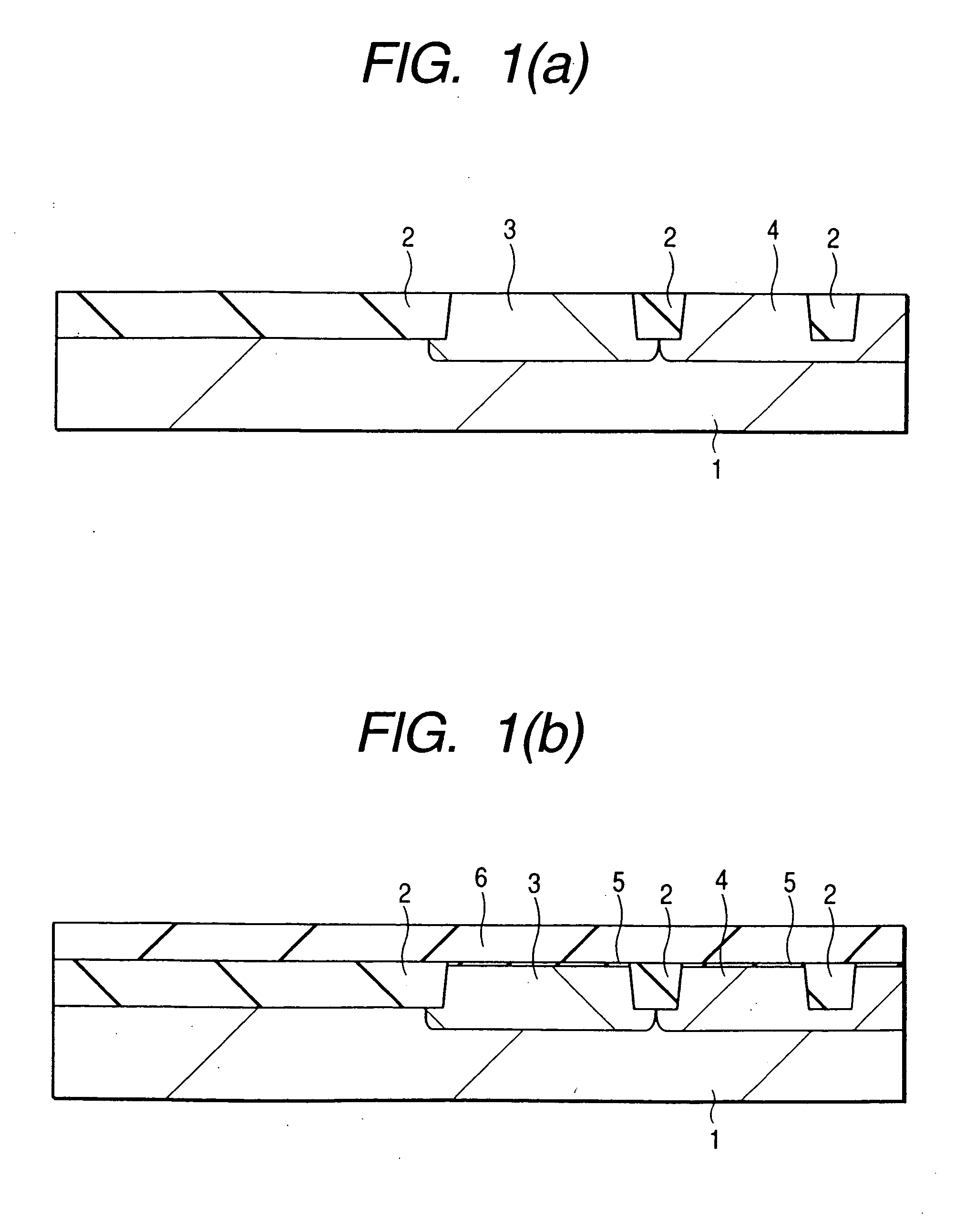
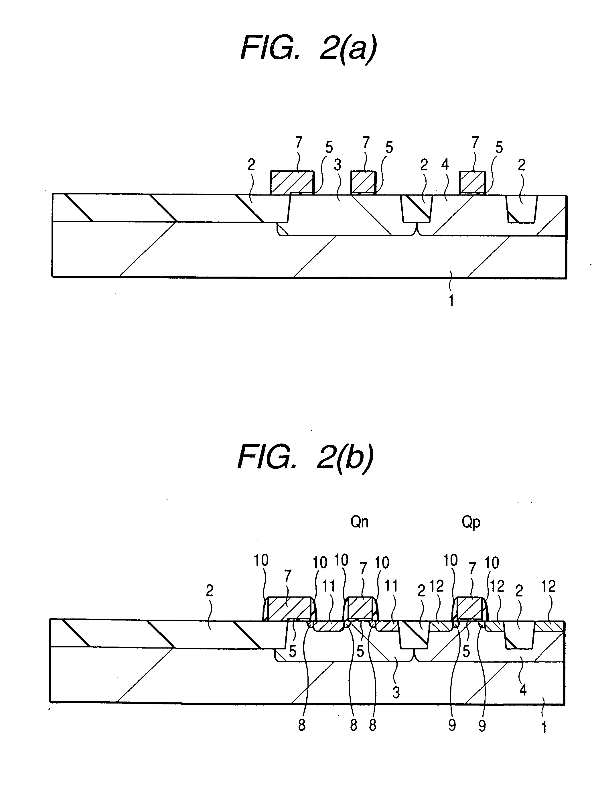
[0063] As shown in FIG. 1a, a semiconductor substrate 1 is made, for example, of p-type single crystal silicon, and an element isolation region 2 is formed on the main surface of the semiconductor substrate 1. For the formation of the element isolation region 2, the semiconductor substrate 1 is etched at the element isolation region thereof to form an approximately 350 nm thick groove, followed by thermal oxidation of the semiconductor substrate 1 at about 850 to 1000° C. to form an approximately 10 nm thick silicon oxide film (not shown) on the inner walls of the groove. Next, a silicon oxide film having a thickness of approximately 45 to 500 nm is deposited on the semiconductor substrate 1, including the inside of the groove, according to a CVD method. Thereafter, the silicon oxide f...

embodiment 2

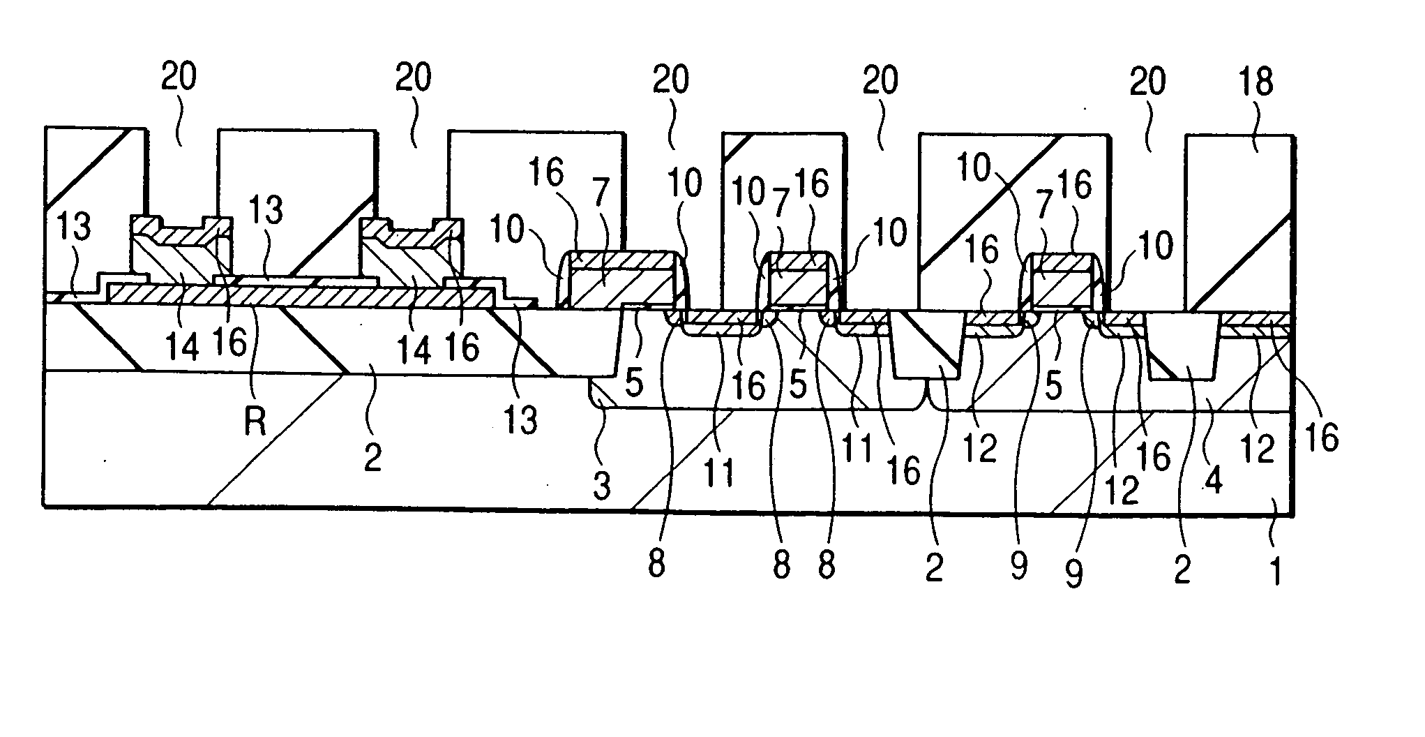
[0118] In Embodiment 1, the wirings are formed according to a so-called single damacene method wherein the wiring is formed at a step different from the step of forming a plug connecting the wirings therewith, but the wirings also may be formed according to a dual damacene method. FIGS. 13 to 20 are, respectively, sectional views showing, one by one, the steps of a method of manufacture of a semiconductor integrated circuit device according to Embodiment 2 of the invention. The steps up to the formation of the plug 21 illustrated with reference to FIG. 1a to FIG. 6a are similar to those of Embodiment 1 and will not be repeatedly described herein.

[0119] The semiconductor substrate 1 shown in FIG. 6a has formed thereon the n-channel MISFET Qn and the p-channel MISFET Qp, which are, respectively, provided with a source and drain having a LDD (lightly doped drain) structure on the p-type well 3 and the n-type well 4, and also is provided with a resistor element including, on the wide e...

embodiment 3

[0155] In Embodiments 1 and 2, after the formation of the tungsten films 26c, 35c (see FIGS. 7b and 9 in Embodiment 1 and FIGS. 15 and 19 in Embodiment 2), the silicon nitride films 28, 36 and the silicon oxide films 29, 37 are formed on the tungsten films 26c, 35c, respectively. Alternatively, as shown in FIGS. 25a and 25b, silicon oxide films (hereinafter referred to as TEOS film ) 328, 336, which are deposited according to a CVD method using tetraethoxysilane as a starting gas, are thinly formed on the tungsten films 26c, 35c, respectively, followed by further formation thereon of insulating films 329, 337 having a dielectric constant lower than the TEOS films (i.e. a dielectric constant of 4 or below). It will be noted that a carbon-containing silicon-based insulating film, such as a silicon carbide film, an SiCO film or the like, may be used in place of the TEOS films 328, 336. The carbon-containing silicon-based insulating film, such as SiC or SiCO, has a dielectric constant a...


PUM

PropertyMeasurementUnit
pressureaaaaaaaaaa
pressureaaaaaaaaaa
thicknessaaaaaaaaaa

Abstract

A barrier layer and a copper film are successively formed on a silicon oxide film including a groove for wiring in the silicon oxide film and a silicon nitride film, both formed on a semiconductor substrate. Thereafter, the barrier layer and the copper film are removed from outside of the groove for wiring, thereby forming a wiring. Tungsten is selectively or preferentially grown on the wiring to selectively form a tungsten film on the wiring. After the formation of the copper film, a treatment with hydrogen may be performed. After the formation of the wiring, the semiconductor substrate may be cleaned with a cleaning solution capable of removing a foreign matter or a contaminant metal. After the formation of the wiring, a treatment with hydrogen is carried out.

Description

[0001] This application is a divisional application of U.S. application Ser. No. 09 / 850,162, filed May 8, 2001, the entire disclosure of which is incorporated herein by reference.[0002] This invention relates to a semiconductor integrated circuit device and also to a method of manufacturing the same. More particularly, the invention relates to a technique which is effective for application to wirings formed by a so-called damascene method wherein, after formation of grooves for wirings in an insulating film, a conductive film is buried inside the grooves. BACKGROUND OF THE INVENTION [0003] In recent years, as advances are being made in the scaling-down and multi-layered formation of wirings in a semiconductor integrated circuit device, a so-called damacene technique has been studied, as described, for example, by T. Saito et. al., in Proceedings of International Interconnect Technology Conference, 1998, pp. 160-162 and the like, in which after formation of a groove for wirings in an...

Claims


Application Information

Patent Timeline
Patent Type & Authority Applications(United States)
IPC IPC(8): H01L21/3205H01L21/28H01L21/4763H01L21/768H01L21/8238H01L23/52H01L27/092
CPCH01L21/28518H01L2224/13H01L21/28562H01L21/76801H01L21/76808H01L21/76834H01L21/76843H01L21/76849H01L21/76861H01L21/76862H01L21/76877H01L21/76882H01L21/76883H01L21/76889H01L23/53295H01L21/2855H01L2224/05001H01L2224/05027H01L2224/05569H01L2224/05024H01L2224/05008H01L2224/05009H01L2224/05022H01L2224/05025H01L2224/05023H01L2224/05572H01L2224/13024H01L21/768
Inventor SAITO, TATSUYUKIOHASHI, NAOHUMIIMAI, TOSHINORINOGUCHI, JUNJITAMARU, TSUYOSHI
Owner RENESAS ELECTRONICS CORP
Why Eureka
Try Eureka