Apparatus and method for shaping high voltage potentials on an insulator

a technology of insulating structure and surface, which is applied in the manufacture of x-ray tubes, electric discharge tubes/lamps, and electromechanical systems, etc., can solve the problems of non-uniform application of coating materials, and achieve the effects of increasing the conductivity of the surface, and increasing the amount of metallic lead

Inactive Publication Date: 2005-05-12
VARIAN MEDICAL SYSTEMS
View PDF14 Cites 2 Cited by
  • Summary
  • Abstract
  • Description
  • Claims
  • Application Information

AI Technical Summary

Benefits of technology

[0015] In a first embodiment, the voltage potential distribution is modified via a coating material non-uniformly applied to the surface of the anode and / or cathode insulator within an x-ray tube. The coating material has an electrical conductivity greater than that of the surface of the insulator. In addition, the coating material is non-uniformly applied in order to adjust the voltage distribution along length of the insulator from the anode or cathode to the vacuum enclosure surface. For instance, the thickness of the coating may be more thickly applied to the surface of the insulator nearest the cathode or anode than it is applied to than the portion nearest the vacuum enclosure surface. Or, the composition of the coating material may be altered such that it possesses greater conductivity where it is applied to the insulator surface nearest the cathode or anode. In this way, the desired voltage potential distribution gradient is achieved along the length of the insulator during operation of the x-ray tube.
[0016] In a second embodiment, the surface of an insulator is modified by preferential reduction of existing material (bulk or trace) using, for example, heating in a hydrogen atmosphere; electron (or ion) beam bombardment; or chemical means. For example, the surface of an anode insulator comprising leaded glass can be modified in order to change its conductivity. In one embodiment, this is accomplished by masking portions of the inner surface of the insulator, typically comprising a funnel or cone shape. The anode insulator is then heated in a furnace having a hydrogen-rich atmosphere, thereby causing a chemical reduction of lead oxide near the insulator surface. This reduction of lead oxide increases the amount of metallic lead near the surface of the insulator, which in turn increases the conductivity of the surface. This process is repeated for different regions of the insulator as desired in order to shape the overall conductivity of the insulator surface. As with the first embodiment, this enhances the ability of the insulator surface to more evenly distribute the voltage potential along the length thereof during tube operation. Similarly, sodium or potassium could be reduced from alumino-ortho-silicate glasses. In other examples, Boron or sodium could be reduced from “Pyrex” glass, or calcium, strontium and other metallic oxides could be reduced from the glassy phase of ceramic materials or from oxide glasses. Preferential reduction of the bulk ceramic material (such as reducing alumina to aluminum, or silicon from silica ceramics) could also be accomplished by similar means.

Problems solved by technology

In addition, the coating material is non-uniformly applied in order to adjust the voltage distribution along length of the insulator from the anode or cathode to the vacuum enclosure surface.

Method used


Image

  • Apparatus and method for shaping high voltage potentials on an insulator
  • Apparatus and method for shaping high voltage potentials on an insulator
  • Apparatus and method for shaping high voltage potentials on an insulator

Examples


first embodiment

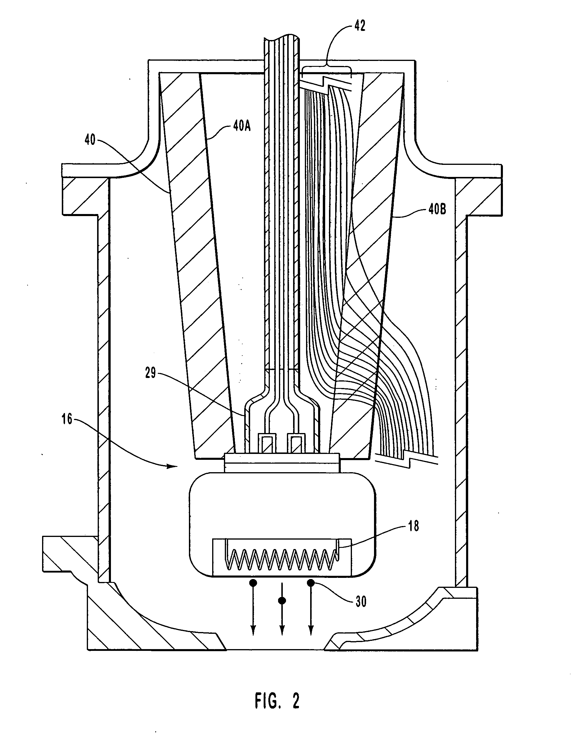
[0038] Attention is now directed to FIG. 3, which depicts a portion of the x-ray tube 10 near the cathode 16. In accordance with the present invention, the outer vacuum surface 40B of the insulating cathode cone 40 has disposed thereon a non-uniform coating material 44. The coating material 44 is used to modify the voltage potential distribution of the electric field along the surface of the cone vacuum surface 40B during tube operation, as explained further below. To that end, the coating material 44 is sufficiently electrically conductive with respect to the insulating material in order to enable it to modify the voltage distribution. Accordingly, the electrically conductive coating material 44 is understood to comprise one of a variety of conductive, semi-conductive, and semi-insulating substances including, but not limited to carbon, silver, copper, nickel, chromium, etc. Alternatively, the coating material 44 could comprise two or more materials applied to the cone vacuum surfa...

second embodiment

[0046] Attention is now directed to FIG. 6, depicting in cross section the anode insulator 68 of the double-ended x-ray tube 60 of FIG. 5. FIG. 6 depicts the anode insulator 68 prepared for use in the x-ray tube 60 in accordance with the present invention. In this embodiment, the surface of the insulating structure itself is modified in a non-uniform manner to enable a more even voltage potential distribution to exist along the surface thereof during tube operation. For example, an anode insulator 68 composed of leaded glass is provided. A first region 72A of the inner vacuum surface 68A remains uncovered while the rest of the inner surface in masked with a heat resistant covering. The anode insulator 68, and particularly the inner vacuum surface 68A, is then fired in a hydrogen-rich atmosphere for a time sufficient to partially chemically alter the unmasked portions of the leaded glass inner vacuum surface 68A in accordance with the following chemical reaction:

PbO2+4H++2e−=Pb2++2H2...

third embodiment

[0050] Reference is now made to FIG. 7, which depicts in cross section the cathode insulator 70 of the double-ended x-ray tube 60 of FIG. 5. FIG. 7 depicts the cathode insulator 70 prepared for use in the x-ray tube 60 in accordance with the present invention. In this embodiment, an electrically conductive pattern is defined on the surface of the insulating structure to create a more even voltage potential distribution along the surface during tube operation.

[0051] As can be seen in the cross sectional view of FIG. 7, the inner vacuum surface of the cathode insulator 70, designated as 70A, has disposed thereon a layer of coating material 80 through which has been scribed a path 82. The coating material 80 is preferably a conductive, semi-conductive, or semi-insulating coating similar to the coating material 44 described in the first embodiment. As such, the coating material 80 may comprise the same materials as the coating material 44, and may be applied using those techniques descr...


PUM


Abstract

An apparatus and method for reducing the incidence of electric field stress on portions of insulating structures within high voltage devices is disclosed. Each of the embodiments disclosed herein modifies the conductive properties of the insulating structure surface in a non-uniform manner such that the distribution of voltage potential along the surface thereof is more fully equalized during operation of the high voltage device. This, in turn, reduces the per unit stress on the insulating structure caused by the electric field of the high voltage device. Though embodiments of the present invention are preferably directed to utilization in x-ray tube devices, a variety of high voltage devices may benefit from application of the disclosed matter.

Description

CROSS-REFERENCE TO RELATED APPLICATIONS [0001] This application is a divisional application, and claims the benefit of U.S. patent application Ser. No. 10 / 378,174, filed Mar. 3, 2003, and entitled APPARATUS AND METHOD FOR SHAPING HIGH VOLTAGE POTENTIALS ON AN INSULATOR, which will issue as U.S. Pat. No. 6,819,741 on Nov. 16, 2004. That application is incorporated herein by reference in its entirety.BACKGROUND OF THE INVENTION [0002] 1. The Field of the Invention [0003] The present invention generally relates to high voltage devices. More particularly, the present invention relates to an apparatus and method for adjusting voltage potentials on the surface of insulating structures used in high voltage devices. [0004] 2. The Relevant Technology [0005] X-ray generating devices are extremely valuable tools that are used in a wide variety of applications, both industrial and medical. For example, such equipment is commonly employed in areas such as medical diagnostic examination, therapeu...

Claims


Application Information

Patent Timeline
Patent Type & Authority Applications(United States)
IPC IPC(8): H01J9/30H01J35/02
CPCH01J35/02H01J9/30
Inventor CHIDESTER, CHARLES LYNN
Owner VARIAN MEDICAL SYSTEMS
Why Eureka
Try Eureka