Method of manufacturing a thin dielectric layer using a heat treatment and a semiconductor device formed using the method

a technology of heat treatment and semiconductor devices, which is applied in the direction of semiconductor devices, electrical equipment, basic electric elements, etc., can solve the problems of high programming voltage, increase manufacturing costs, and increase the size of the thick layer, so as to reduce the size of the transistor and the resulting storage cell, the effect of increasing the capacitance coupling

Active Publication Date: 2005-05-19
SAMSUNG ELECTRONICS CO LTD
View PDF13 Cites 6 Cited by
  • Summary
  • Abstract
  • Description
  • Claims
  • Application Information

AI Technical Summary

Benefits of technology

[0011] In one embodiment, the thin dielectric layer comprises an inter-gate dielectric layer, the lower conductive layer comprises a floating gate and the upper dielectric layer comprises a control gate of a transistor, for example, a non-volatile memory cell transistor. In this manner, the thin dielectric layer provides for increased capacitive coupling between the lower floating gate and the upper control gate. This also leads to a lowered programming voltage, erasing voltage and read voltage for the transistor, while maintaining the threshold voltage in a desired range. In addition, the size of the transistor and resulting storage cell can be minimized and the need for a high-voltage region in the circuit is mitigated, since, assuming a lowered programming voltage, pumping circuitry is not required.
[0012] The thin dielectric layer is formed using a heat treatment process that results in a reduction of surface roughness of the underlying floating gate and results in a thin silicon oxy-nitride layer being formed on the floating gate. A dielectric layer is formed on the silicon oxy-nitride layer, and the combined layers form an inter-gate dielectric layer. The resulting thin dielectric layer is an excellent barrier to charge migration from the floating gate.
[0016] In one embodiment, the first heat treatment improves surface roughness in an upper surface of the first conductive layer. The second heat treatment provides an oxy-nitride interface on the first conductive layer. The oxy-nitride interface comprises, for example, silicon oxy-nitride SiOxNy material, and is less than about 20 Å in thickness. In one embodiment, the combined thickness of the oxy-nitride interface and the dielectric layer is less than about 70 Å in thickness.

Problems solved by technology

Such large-scale components tend to consume valuable chip surface area, and tend to raise the manufacturing costs.
Such a thick layer requires an excessively high programming voltage to ensure capacitive coupling between the control gate and the floating gate.
However, nitride does not adhere well to the polysilicon material in the control gate and floating gate and therefore is impractical for use alone as an inter-gate dielectric material.

Method used


Image

  • Method of manufacturing a thin dielectric layer using a heat treatment and a semiconductor device formed using the method
  • Method of manufacturing a thin dielectric layer using a heat treatment and a semiconductor device formed using the method
  • Method of manufacturing a thin dielectric layer using a heat treatment and a semiconductor device formed using the method

Examples


Embodiment Construction

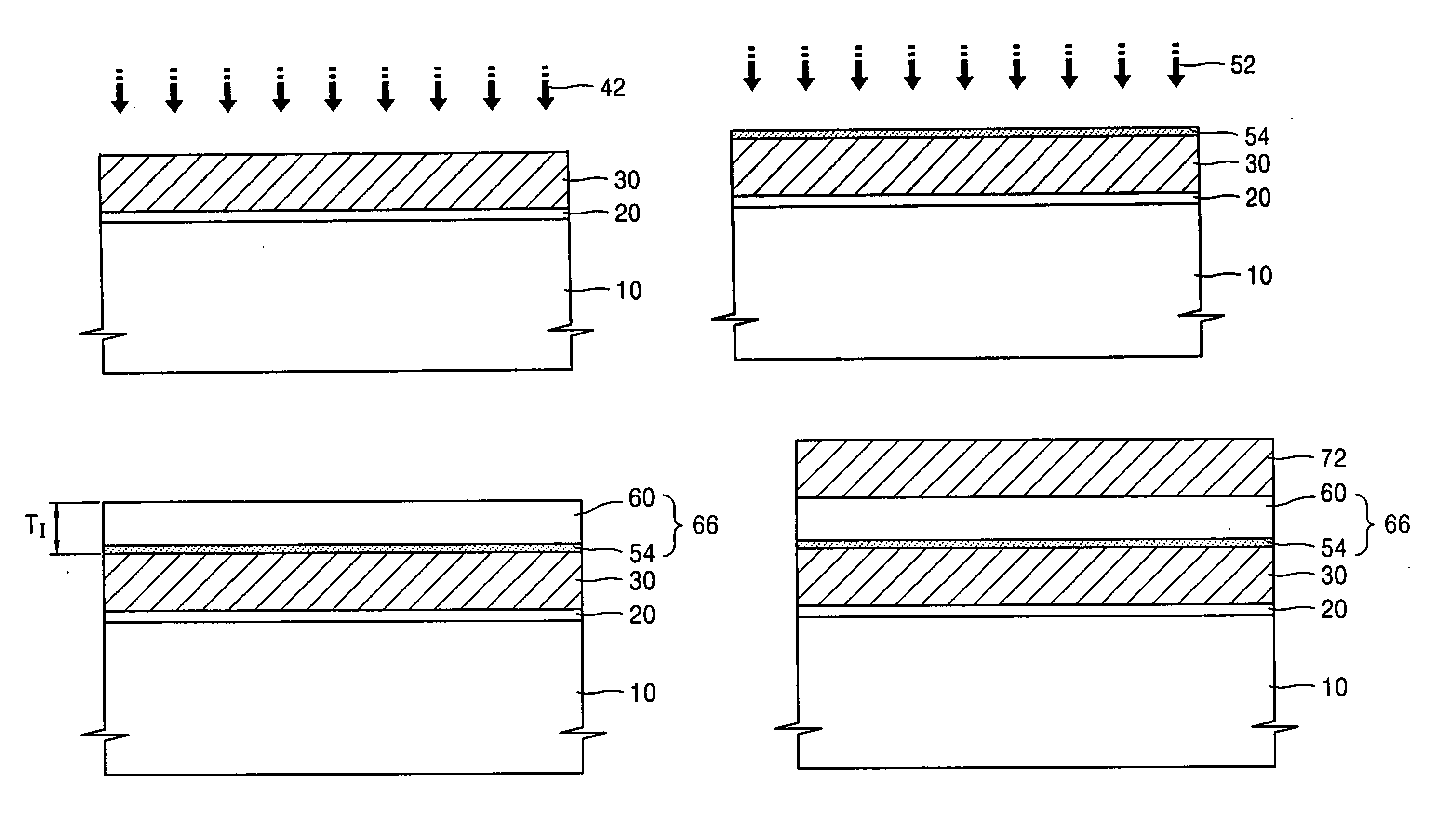
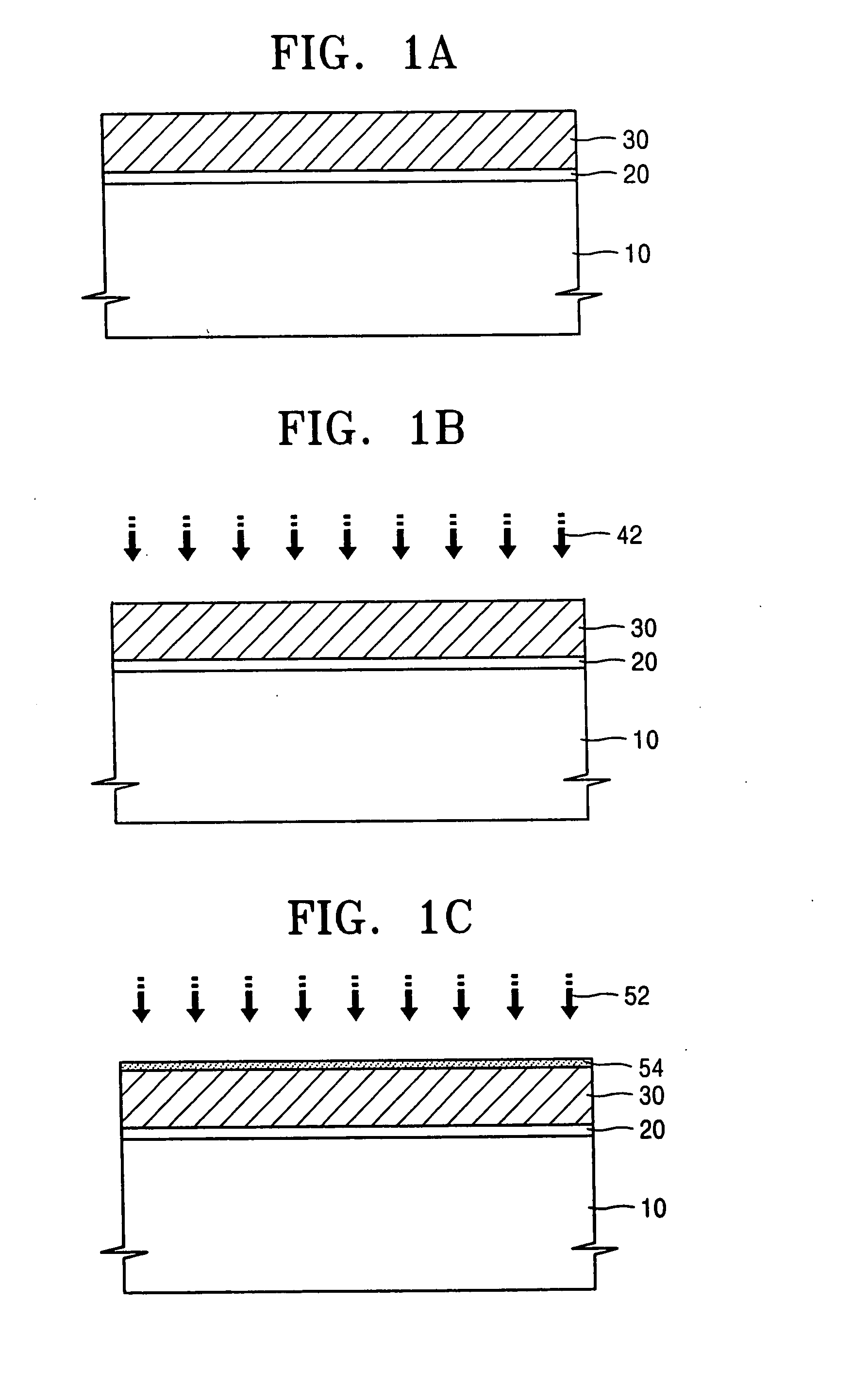
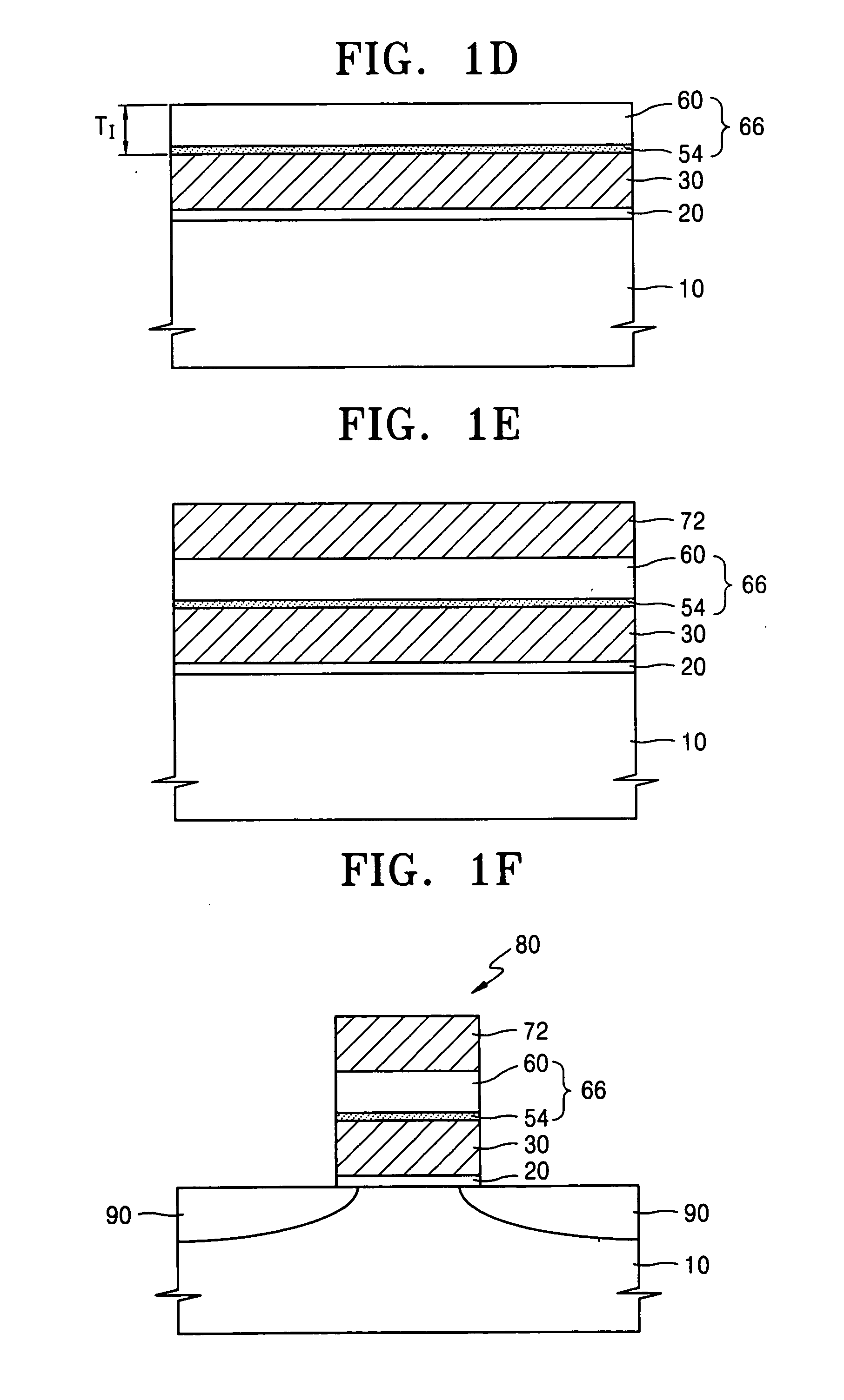
[0028] In the following description of preferred embodiments of the present invention and in the claims that follow, the term “on”, when referring to layers of material used in the fabrication of semiconductor devices, refers to a layer that is directly applied to an underlying layer, or refers to a layer that is above an underlying layer with an optional intermediate layer or layers therebetween. The thicknesses of the respective layers are not necessarily to scale in the drawings, but instead are exaggerated for clarity and to illustrate the various features of the present invention.

[0029]FIGS. 1A-1F are cross-sectional views of the fabrication of a semiconductor device in accordance with an embodiment of the present invention.

[0030] In FIG. 1A, a gate insulating layer 20 is formed to a thickness of 100 Å on a semiconductor substrate 10. In one embodiment, the semiconductor substrate comprises silicon material and the gate insulating layer comprises SiO2, or “oxide”.

[0031] A fi...


PUM


Abstract

In a method for forming a semiconductor device and a semiconductor device formed in accordance with the method, a thin dielectric layer is provided between a lower conductive layer and an upper conductive layer. In one embodiment, the thin dielectric layer comprises an inter-gate dielectric layer, the lower conductive layer comprises a floating gate and the upper dielectric layer comprises a control gate of a transistor, for example, a non-volatile memory cell transistor. The thin dielectric layer is formed using a heat treating process that results in reduction of surface roughness of the underlying floating gate, and results in a thin silicon oxy-nitride layer being formed on the floating gate. In this manner, the thin dielectric layer provides for increased capacitive coupling between the lower floating gate and the upper control gate. This also leads to a lowered programming voltage, erasing voltage and read voltage for the transistor, while maintaining the threshold voltage in a desired range. In addition, the size of the transistor and resulting storage cell can be minimized and the need for a high-voltage region in the circuit is mitigated, since, assuming a lowered programming voltage, pumping circuitry is not required.

Description

RELATED APPLICATIONS [0001] This application claims priority to Korean Patent Application Serial Number 2003-80574, filed Nov. 14, 2003, the contents of which are incorporated herein by reference, in their entirety. BACKGROUND OF THE INVENTION [0002] Non-volatile memory devices find widespread application in electronic systems that do not receive continuous power, for example in applications where power is not always available, where power is frequently interrupted, and / or where low-power usage is desired. Example applications include mobile telecommunication systems, memory cards for storing music and / or image data, and system-on-a-chip applications that include a processing unit and a memory unit. [0003] Cell transistors in non-volatile memory devices commonly employ a stacked gate structure that is formed over a channel region of a substrate between source / drain regions. The stacked gate structure includes a sequentially stacked gate insulating layer formed on the channel, floati...

Claims


Application Information

Patent Timeline
Patent Type & Authority Applications(United States)
IPC IPC(8): H01L21/28H01L21/314H01L27/115
CPCH01L21/3144H01L21/28273H01L29/40114H01L21/0214H01L21/02249H01L21/02252H10B69/00
Inventor KANG, SUNG-TAEGHAN, JEONG-UKPARK, SUNG-WOOYOON, SEUNG-BEOMPARK, JI-HOONSEO, BO-YOUNG
Owner SAMSUNG ELECTRONICS CO LTD
Why Eureka
Try Eureka