

OLEDs having n-type doping
a technology of n-type and n-type, applied in the direction of discharge tube luminescnet screen, other domestic articles, natural mineral layered products, etc., can solve the problems of limiting the conductivity of the layer, low number of charge carriers, and doping with li
- Summary
- Abstract
- Description
- Claims
- Application Information
AI Technical Summary
Problems solved by technology
Method used
Image

Examples
example 1
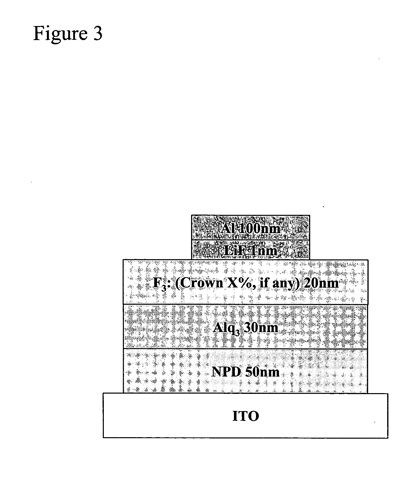
[0108] Two devices were prepared, ITO / NPD (500 Å) / Alq3 (300 Å) / F3 (200 Å) / Li (10 Å) / Al (1000 Å) and ITO / NPD (500 Å) / Alq3 (300 Å) / F3+15% DBC (200 Å) / Li (10 Å) / Al (1000 Å). The organic light emitting devices were grown on a glass substrate pre-coated with a ˜100-nm thick layer of indium-tin-oxide (ITO) having a sheet resistance of ˜20 Ω / □. Substrates were cleaned with solvents and then cleaned by exposure to UV-ozone ambient for 10 minutes. After cleaning, the substrates were immediately loaded into a thermal evaporation system operating at a base pressure of ˜1×10⁻⁶ Torr. A 500-Å-thick 4-4′-bis[N-(1-naphthyl)-N-phenyl-amino]biphenyl (α-NPD) hole transport layer (HTL) was deposited. Next, a 300-Å-thick aluminum (III) tris (8-hydroxyquinoline) (Alq3) as emitting material was deposited. Dibenzo-18-crown-6 (15% by weight) was co-deposited with fluorene trimer (F3) to form the 300-Å-thick electron transport layer (ETL) and in the reference device only F3 was deposited as ETL. Device catho...
example 2
[0111] Devices were prepared having the structure ITO / NPD (500 Å) / Alq3 (300 Å) / F3 (200 Å) / Li (10 Å) / Al (1000 Å) and ITO / NPD (500 Å) / Alq3 (300 Å) / ETL (200 Å) / Li (10 Å) / Al (1000 Å), in which ETL is (i) 5% DBC in F3, (ii) 15% DBC in F3, (iii) 25% DBC in F3, or (iv) F3 alone. Organic light emitting devices were grown on a glass substrate pre-coated with a ˜100-nm thick layer of indium-tin-oxide (ITO) having a sheet resistance of ˜20 Ω / □. Substrates were cleaned with solvents and then cleaned by exposure to UV-ozone ambient for 10 minutes. After cleaning, the substrates were immediately loaded into a thermal evaporation system operating at a base pressure of ˜1×10⁻⁶ Torr. A 500-Å-thick 4-4′-bis[N-(1-naphthyl)-N-phenyl-amino]biphenyl (α-NPD) hole transport layer (HTL) was deposited. Next, a 300-Å-thick aluminum (III) tris (8-hydroxyquinoline) (Alq3) as emitting material was deposited. In three separate devices, a 300-Å-thick electron transport layer (ETL), consisting of X % (X %=5%, 15% a...
example 3
[0113] Devices were prepared having the structures (A) ITO / NPD (400 Å) / mCP(100 Å) / 10% Ir(4,6-F2 ppy)2(BPZ4): p-(SiPh3)2Ph (250 Å) / F3 (200 Å) / 15% F3:DBC (100 Å) / LiF / Al (1000 Å), and (B) ITO / NPD (400 Å) / 10% Ir(4,6-F2 ppy)2(BPz4): p-(SiPh3)2Ph (250 Å) / F3 (200 Å) / 15% F3:DBC (100 Å) / LiF / Al (1000 Å) (FIGS. 12A and 12B). The organic light emitting devices were grown on a glass substrate pre-coated with a ˜100-nm thick layer of indium-tin-oxide (ITO) having a sheet resistance of ˜20 Ω / □. Substrates were cleaned with solvents and then cleaned by exposure to UV-ozone ambient for 10 minutes. After cleaning, the substrates were immediately loaded into a thermal evaporation system operating at a base pressure of ˜1×10⁻⁶ Torr. A 500-Å-thick 4-4′-bis[N-(1-naphthyl)-N-phenyl-amino]biphenyl (α-NPD) hole transport layer (HTL) was deposited. In one device a 100 Å thick layer of mCP was deposited. Next a 250-Å-thick phosphorescent emissive layer of 10% Ir(4,6-F2 ppy)2(BPz4) in p-(SiPh3)2Ph (250 Å) was ...
PUM
 Abstract
Description
Claims
Application Information