Fabrication method for semiconductor device and manufacturing apparatus for the same

a manufacturing apparatus and semiconductor technology, applied in semiconductor devices, furnace types, furnaces, etc., can solve the problems of deterioration of the morphology of the surface layer of the semiconductor substrate after activation, inability to obtain the desired impurity profile, and interference by multiphoton processes

Active Publication Date: 2005-06-09
KIOXIA CORP
View PDF3 Cites 20 Cited by
  • Summary
  • Abstract
  • Description
  • Claims
  • Application Information

AI Technical Summary

Benefits of technology

[0014] Another aspect of the present invention inheres in a fabrication method for a semiconductor device, including: forming the device isolation regions on the semiconductor substrate; forming a gate electrode in the device regions, which is partitioned by the device isolation regions, via a gate insulator layer; forming impurity ion implanted layers in the source and the drain extension region using the gate electrode as a mask; depositing a silicon oxide film on the surface of the substrate at a low temperature; removing excessive silicon oxide film from the semiconductor substrate; processing the substrate so that the silicon oxide film remains only on a sidewalls of the gate electrode; forming impurity ion implanted layers in the source and the drain region using the gate electrode and the silicon oxide film remaining on the sidewalls thereof as a mask; performing a first annealing for the semiconductor substrate by light irradiation using a flash lamp with a first energy density after forming the impurity ion implanted layers in the source and the drain region; and performing a second annealing for the semiconductor substrate by light irradiation using a flash lamp with a second energy density after performing the first annealing.
[0015] Another aspect of the present invention inheres in a fabrication method for a semiconductor device, including: forming the device isolation regions on the semiconductor substrate; forming a gate electrode in the device regions, which is partitioned by the device isolation regions, via a gate insulator layer; forming impurity ion implanted layers in the source and the drain extension region using the gate electrode as a mask; depositing a silicon oxide layer on the surface of the substrate at a low temperature; removing excessive silicon oxide film from the semiconductor substrate; processing the substrate so that the silicon oxide film remains only on a sidewalls of the gate electrode; forming impurity ion implanted layers in the source and the drain region using the gate electrode and the silicon oxide film remaining on the sidewalls thereof as a mask; performing a first annealing for the semiconductor substrate using a tungsten halogen lamp after formation of the impurity ion implanted layers in the source and the drain region; and performing a second annealing for the semiconductor substrate using a flash lamp after performing the first annealing.

Problems solved by technology

In recent years, a desired impurity profile cannot be obtained, since impurity diffusion occurs even after performing the annealing for a short time.
However, since a laser light inherently has high coherency and directivity, a multiphoton process or interference may occur.
Therefore, the morphology of a surface layer of a semiconductor substrate will be deteriorated after activation.
In addition, when the annealing temperature is reduced, there is a problem that the activation rate of impurities drastically declines.
Accordingly, it is difficult to form a shallow impurity diffusion layer with a junction depth of less than 50 nm and with low resistivity.
However, with FLA which performs annealing in a matter of milliseconds, it is difficult to sufficiently fix crystal defects, which are developed in the semiconductor substrate during the ion implantation process.
Immediately after the ion implantation process, a crystal structure in a region where dopant is implanted in the semiconductor substrate is partially damaged and turns into an amorphous layer.
If a large amount of crystal defects remain in, for example, the source and the drain region, those crystal defects may develope into a conductive path.
This may cause an increase in leakage current during transistor operation, resulting in deterioration in the characteristics.
However, in this case, it is difficult to form a shallow junction since the impurities will deeply diffuse.

Method used


Image

  • Fabrication method for semiconductor device and manufacturing apparatus for the same
  • Fabrication method for semiconductor device and manufacturing apparatus for the same
  • Fabrication method for semiconductor device and manufacturing apparatus for the same

Examples


first embodiment

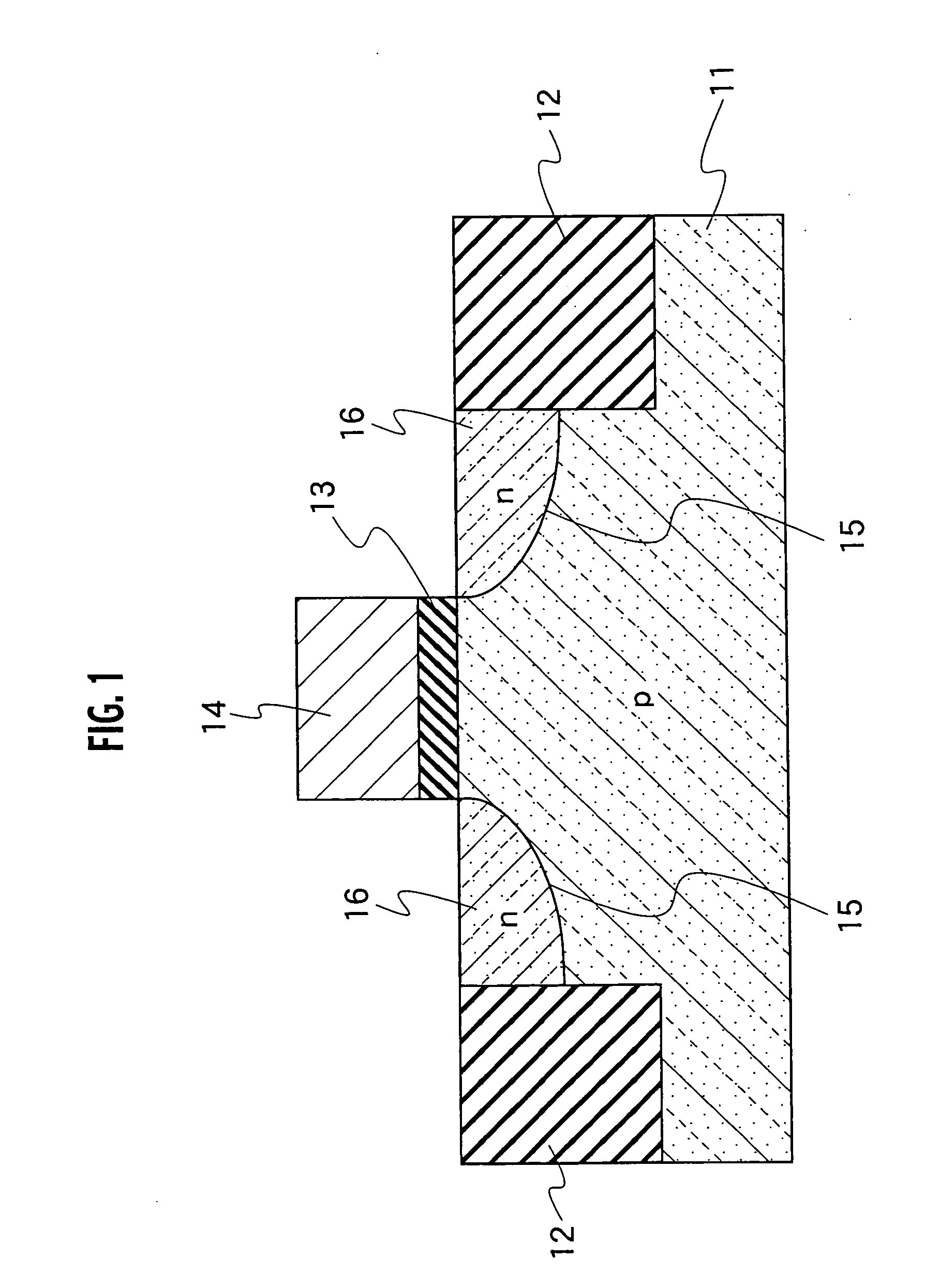
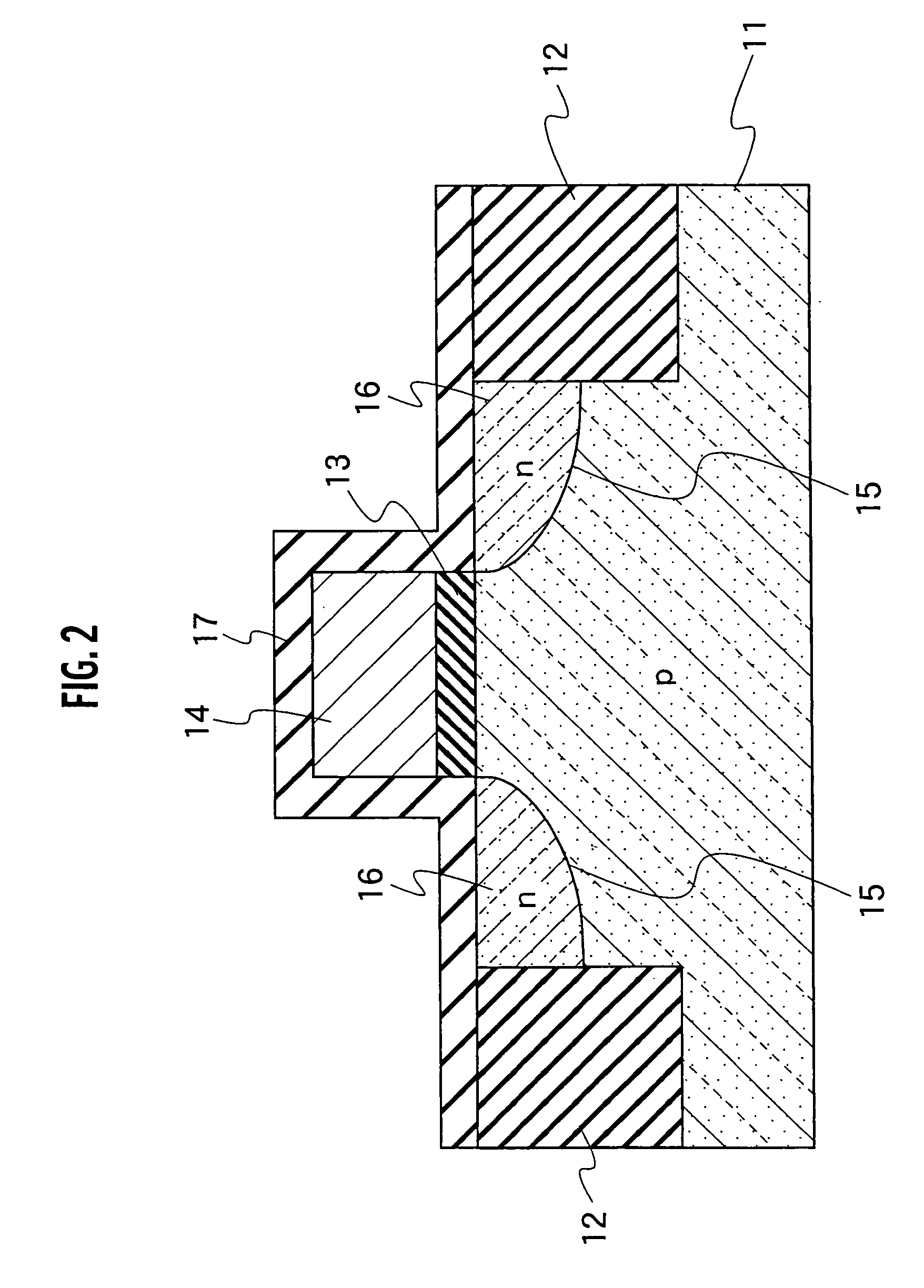
[0037] A semiconductor device manufactured using a semiconductor device fabrication method according to a first embodiment of the present invention is, for example, a metal oxide semiconductor (MOS) field effect transistor, as shown in FIG. 6, configured with a semiconductor substrate 11, device isolation regions 12, a source and a drain region 18, a source and a drain extension region 15, a gate insulator layer 13, a gate electrode 14, and silicon oxide films 17, which are disposed on the sidewalls of the gate electrode 14. In FIG. 6, a source and a drain electrode are omitted. FIGS. 1 through 6 are cross-sectional process diagrams for describing a semiconductor device fabrication method according to the first embodiment of the present invention.

[0038] To begin with, the device isolation regions 12 formed with STIs (shallow trench isolation) or the like are formed on the semiconductor substrate 11 made of, for example, a monocrystalline silicon using an ordinary MOS transistor fab...

second embodiment

[0048] A semiconductor device manufactured using a semiconductor device fabrication method according to a second embodiment of the present invention is a MOS field effect transistor, which is configured with a semiconductor substrate 11, device isolation regions 12, a source and a drain region 18, a source and a drain extension region 15, a gate insulator layer 13, a gate electrode 14, silicon oxide films 17 disposed on the sidewalls of the gate electrode 14, and ion implanted layers 16 and 19, as shown in FIG. 8, for example. In FIG. 8, a source and a drain electrode are omitted. The structure shown in FIG. 8 is substantially the same as that shown in FIG. 6. However, since RTA processing is performed in place of the first FLA, a higher activation rate of the implanted ions in the ion implanted layers 16 and 19 is expected. A diffusion layer tends to extend deeper due to the RTA processing.

[0049] The semiconductor device fabrication method according to the second embodiment of the...

third embodiment

[0064] As with the second embodiment, a semiconductor device manufactured using a semiconductor device fabrication method according to a third embodiment of the present invention is a MOS field effect transistor, which is configured with a semiconductor substrate 11, device isolation regions 12, a source and a drain region 18, a source and a drain extension region 15, a gate insulator layer 13, a gate electrode 14, silicon oxide films 17, which are disposed on the sidewalls of the gate electrode 14, and ion implanted layers 16 and 19, as shown in FIG. 8, for example. In FIG. 8, a source and a drain electrode are omitted. In the third embodiment, as shown in FIG. 11, since the first FLA processing is performed in the annealing process for the activation of implanted ions (11), which begins immediately after the impurity doping process 1, a higher activation rate of implanted ions with the impurity doping process 1 is expected. The structure shown in FIG. 8 is substantially the same a...


PUM


Abstract

A shallow p-n junction diffusion layer having a high activation rate of implanted ions, low resistivity, and a controlled leakage current is formed through annealing. Annealing after impurities have been doped is carried out through light irradiation. Those impurities are activated by annealing at least twice through light irradiation after doping impurities to a semiconductor substrate 11. The light radiations are characterized by usage of a W halogen lamp RTA or a flash lamp FLA except for the final light irradiation using a flash lamp FLA. Impurity diffusion maybe controlled to a minimum, and crystal defects, which have developed in an impurity doping process, may be sufficiently reduced when forming ion implanted layers in a source and a drain extension region of the MOSFET or ion implanted layers in a source and a drain region.

Description

CROSS REFERENCE TO RELATED APPLICATIONS [0001] This application is based upon and claims the benefit of priority from the prior Japanese Patent Application No. P2003-376940 filed on Nov. 6, 2003, the entire contents of which are incorporated herein by reference. BACKGROUND OF THE INVENTION [0002] 1. Field of the Invention [0003] The present invention relates to a fabrication method for a semiconductor device and a manufacturing apparatus for the same. [0004] 2. Description of the Related Art [0005] In order to improve large scale integrated circuit (LSI) performance, the integrated density or miniaturization of the elements used to configure an LSI has been enhanced. In order to miniaturize elements, reduction in the area of an impurity diffusion region as well as formation of a shallower diffusion region along the depth of the diffusion are required. For that purpose, it has become important to optimize ion implantation, which forms an impurity diffusion region such as a source and...

Claims


Application Information

Patent Timeline
Patent Type & Authority Applications(United States)
IPC IPC(8): H01L21/265H01L21/324H01L21/336H01L29/78
CPCH01L21/26533H01L29/6659H01L21/324
Inventor ITANI, TAKAHARUITO, TAKAYUKISUGURO, KYOICHI
Owner KIOXIA CORP
Why Eureka
Try Eureka