Monodisperse core/shell and other complex structured nanocrystals and methods of preparing the same

Active Publication Date: 2005-06-16
THE BOARD OF TRUSTEES OF THE UNIV OF ARKANSAS
View PDF9 Cites 241 Cited by
  • Summary
  • Abstract
  • Description
  • Claims
  • Application Information

AI Technical Summary

Benefits of technology

[0120] In yet another aspect, the present invention provides synthetic methods for preparing high quality, highly monodisperse core/shell and other complex structured nanocrystals. In this aspect, for example, the methods of this invention allow a narrow size distribution of core/shell nanocrystals to be attained as the growth of a shell material proceeds.
[0121] The synthetic methods of the present invention provide for preparing high quality, nearly monodisperse core/shell and other complex structured nanocrystals. In this aspect, for example, the methods of this invention allow a narrow size distribution of core/shell nanocrystals to be attained as the growth of a shell material proceeds. While not intending to be bound by theory, it is believed t

Problems solved by technology

However, plain core nanocrystals may suffer from lack of stability and processability.
While not intending to be bound by theory, it is possible that the underlying causes of this instability and poor processability may be intrinsic.
Further, plain core nanocrystals may also be chemically and thermally less stable than a corresponding core/shell nanocrystal comprising a core of the same composition

Method used


Image

  • Monodisperse core/shell and other complex structured nanocrystals and methods of preparing the same
  • Monodisperse core/shell and other complex structured nanocrystals and methods of preparing the same
  • Monodisperse core/shell and other complex structured nanocrystals and methods of preparing the same

Examples


example 1

Synthesis of CdSe Core Nanocrystals

[0388] Highly fluorescent CdSe nanocrystals were prepared as described in the following typical reaction. A mixture of 0.2 mmol (25.6 mg) of CdO, 0.8 mmol (227 mg) of stearic acid, and 2 g of ODE was prepared in a 25 mL, three-necked flask, and this mixture was heated to about 200° C. to form a clear, colorless solution. The solution was then cooled to room temperature, and 1.5 g of ODA and 0.5 g of TOPO were subsequently added. Under an argon flow, this mixture was reheated to 280° C. A selenium stock solution, prepared by dissolving 2 mmol (158 mg) of Se in 0.472 g of TBP and diluting the solution with 1.37 g of ODE, was quickly injected at this injection temperature of 280° C. The mixture was then maintained at the growth temperature of 250° C. until the desired size of the nanocrystals was obtained.

[0389] This reaction generated CdSe nanocrystals of about 3.5 nm in size, characterized by having a first absorption peak around 570 nm. The reac...

example 2

Synthesis of Cadmium (Cation Precursor) and Sulfur (Anion Precursor) Injection Solutions

[0390] Synthesis of the cadmium sulfide shell material for various core / shell nanocrystals, for example, the CdSe / CdS core / shell nanocrystals, was accomplished at relatively low temperatures by using the following injection solutions for the cation precursor cadmium and the anion precursor sulfur, respectively. The cadmium injection solution (0.04 M) was prepared by dissolving CdO (0.615 g) in oleic acid (OA, 10.83 g), and 1-octadecene (ODE, 108 mL), at 250° C. The sulfur injection solution (0.04 M) was prepared by dissolving sulfur in ODE at 200° C. Both injection solutions were prepared under an argon flow. After clear solutions were obtained, the cadmium injection solution was allowed to cool to about 60° C. for use, while the sulfur injection solution was allowed to cool to room temperature for use. For each injection, a calculated amount of a given injection solution was taken with a syrin...

example 3

Calculations for the Injection Procedure Using the Cadmium and Sulfur Injection Solutions

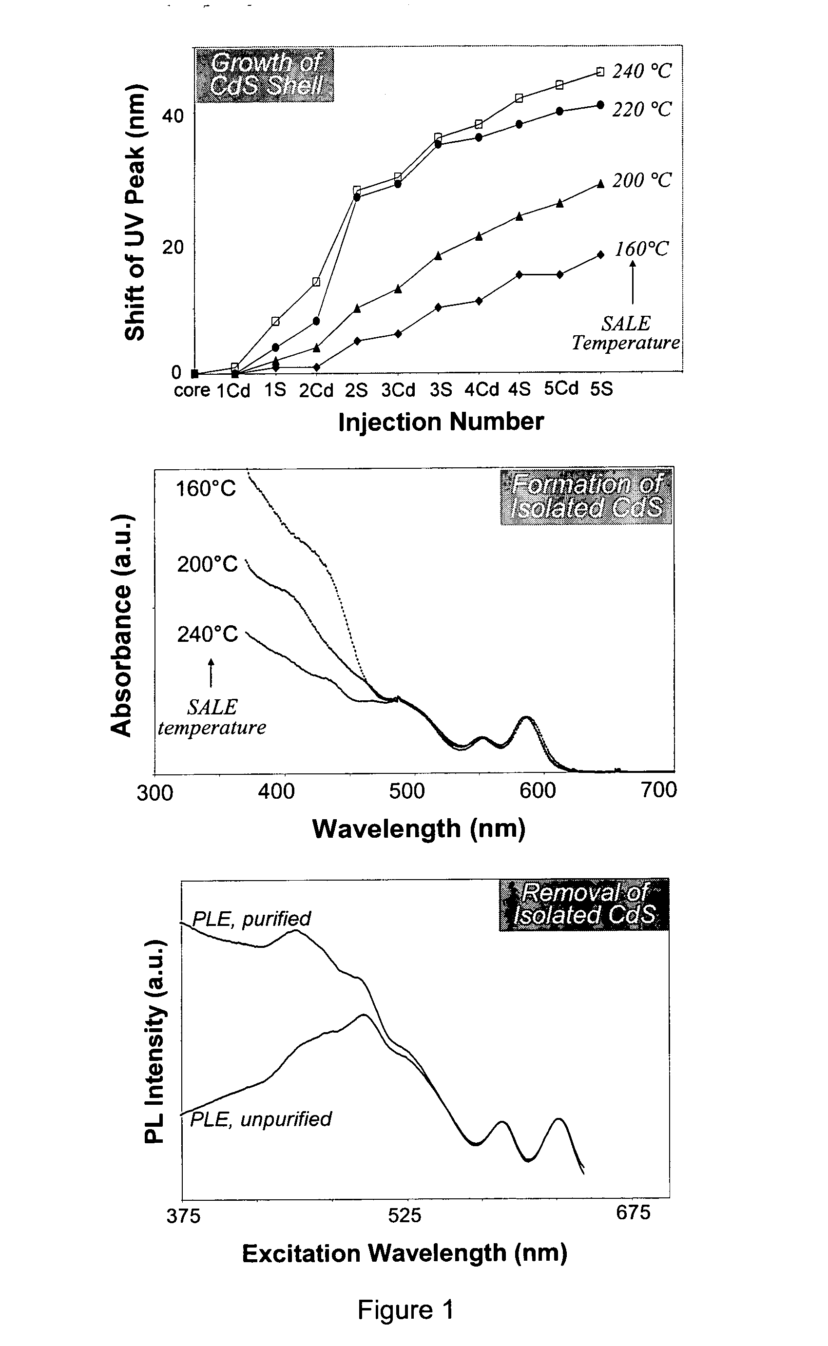
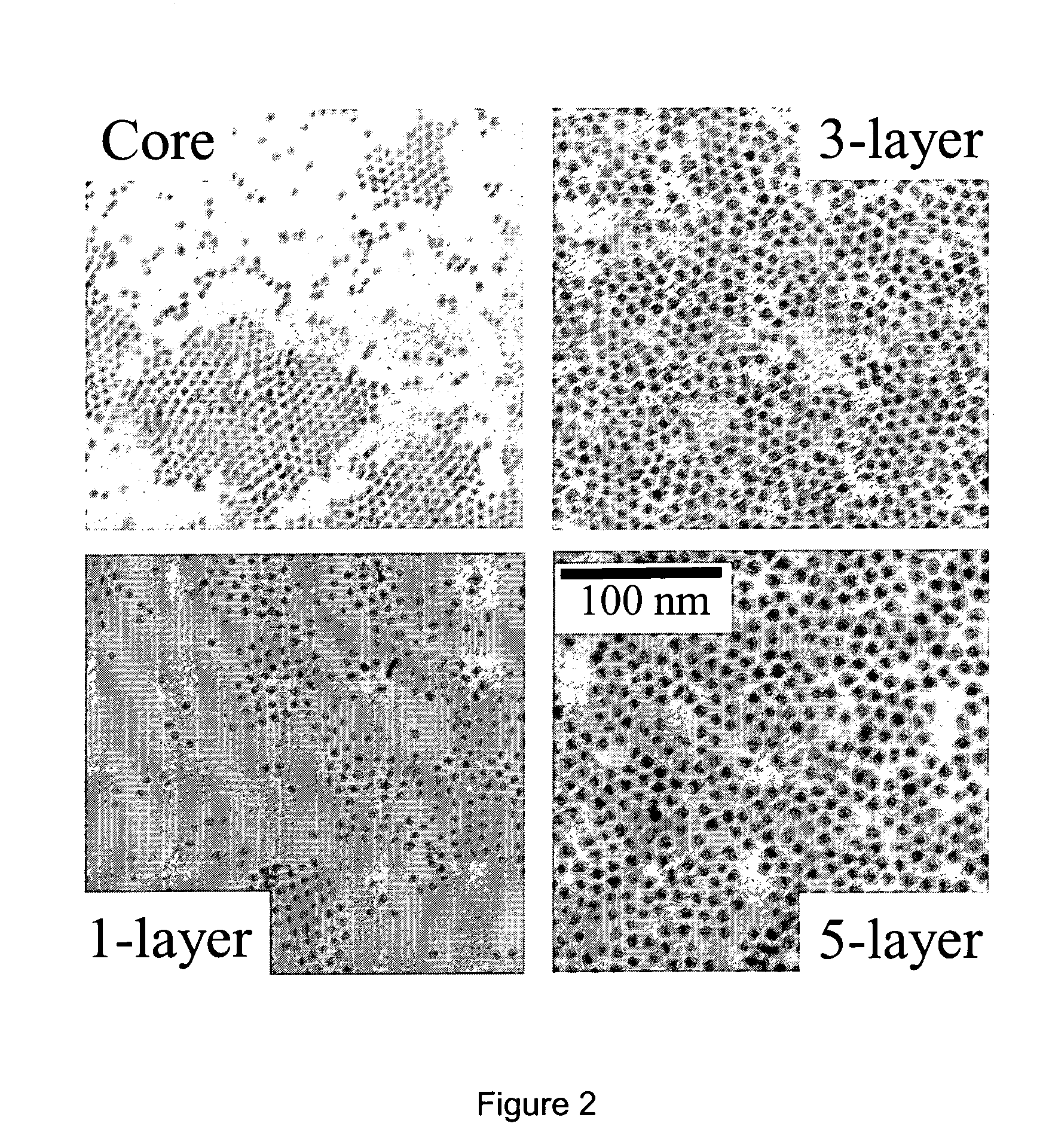
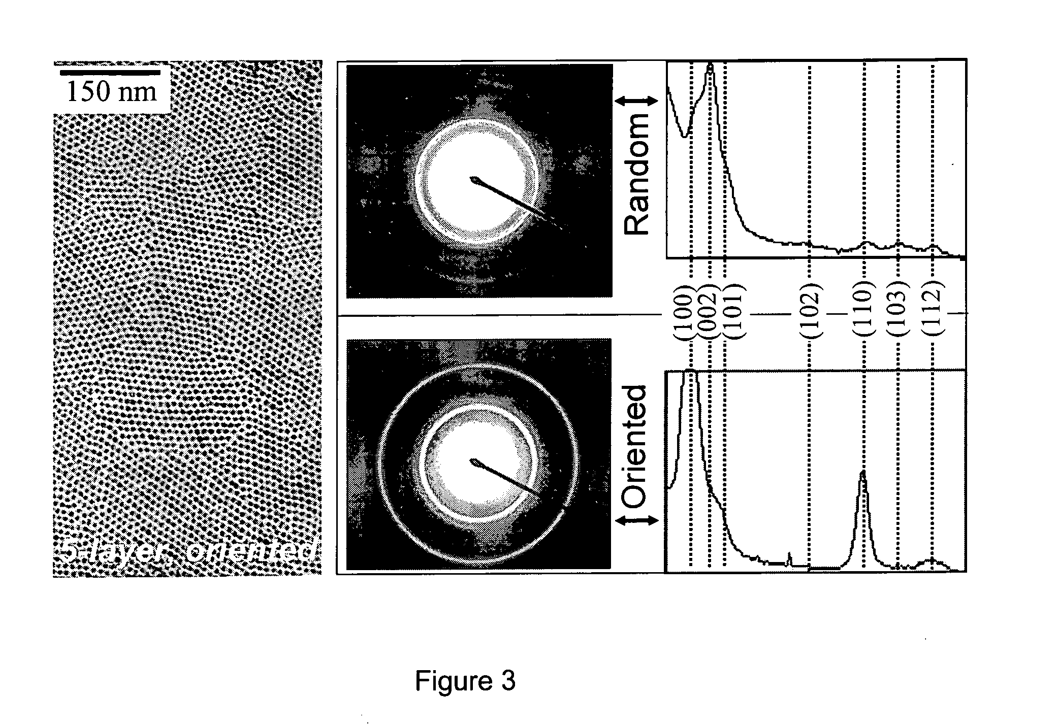
[0391] The successive ionic layer adsorption and reaction (SILAR) technique employed herein, also termed the solution atomic layer epitaxy (SALE) technique, was based on the alternating injections of the cation injection solution and the anion injection solution, into a solution containing the core nanocrystals. For example, as applied to the growth of CdSe / CdS core / shell nanocrystals, the SILAR technique disclosed herein was based on the alternating injections of the Cd injection solution and the S injection solution, into a solution containing CdSe nanocrystals.

[0392] The amount of cadmium or sulfur, and hence the amount of injection solution, needed for each layer was determined by calculating the number of surface atoms of a given sized core / shell nanocrystal. Since there is only about a 5-6% lattice mismatch between CdSe and CdS bulk crystals, the calculations were based on the wurtzite ...


PUM

PropertyMeasurementUnit
Fractionaaaaaaaaaa
Fractionaaaaaaaaaa
Fractionaaaaaaaaaa

Abstract

The present invention provides new compositions containing naearly monodisperse colloidal core/shell semiconductor nanocrystals with high photoluminescence quantum yields (PL QY), as well as other complex structured semiconductor nanocrystals. This invention also provides new synthetic methods for preparing these nanocrystals, and new devices comprising these compositions. In addition to core/shell semiconductor nanocrystals, this patent application also provides complex semiconductor nanostructures, quantum shells, quantum wells, doped nanocrystals, and other multiple-shelled semiconductor nanocrystals.

Description

PRIOR RELATED U.S. APPLICATION DATA [0001] This application claims priority to U.S. patent application Ser. No. 60 / 442,146, filed Jan. 22, 2003, which is incorporated by reference herein in its entirety.STATEMENT OF GOVERNMENT LICENSE RIGHTS [0002] The inventors received partial funding support through the National Science Foundation (Grant No. CHE0101178) and support through the joint Oklahoma University-University of Arkansas Center for Semiconductor Physics in Nanostructures. The Federal Government may retain certain license rights in this invention.TECHNICAL FIELD OF THE INVENTION [0003] The present invention relates to semiconductor nanocrystalline materials and to methods of making and using such materials. BACKGROUND OF THE INVENTION [0004] Colloidal semiconductor nanocrystals are nanometer-sized fragments of the corresponding bulk crystals, which have generated fundamental interest for their promise in developing advanced optical materials. The size-dependent emission is pro...

Claims


Application Information

Patent Timeline
IPC IPC(8): B32B1/00C09K11/02C09K11/08C09K11/56C09K11/70C09K11/74C09K11/88C30B7/00C30B29/60G01N33/58H01L33/18H01L33/28H01S5/30H05B33/14
CPCB82Y15/00Y10T428/2991C09K11/02C09K11/565C09K11/703C09K11/7414C09K11/883C30B7/00C30B29/605G01N33/588H01L31/0352H01L31/036H01L33/18H01L33/28H01S3/169H01S5/30B82Y30/00C09K11/025C09K11/7492
Inventor PENG, XIAOGANGLI, JAINQINGBATTAGLIA, DAVIDWANG, Y. ANDREWWANG, YUNJUN
Owner THE BOARD OF TRUSTEES OF THE UNIV OF ARKANSAS
Why Eureka
Try Eureka