Field effect transistor and manufacturing method thereof

a manufacturing method and transistor technology, applied in the direction of luminescent compositions, semiconductor devices, chemistry apparatus and processes, etc., can solve the problems of difficult to actually change the physical properties of the bulk, large change of electron density, and variable problems to be solved

Inactive Publication Date: 2005-06-30
HITACHI LTD
View PDF5 Cites 40 Cited by
  • Summary
  • Abstract
  • Description
  • Claims
  • Application Information

AI Technical Summary

Benefits of technology

[0048]FIG. 24 is a cross-sectional view showing a manufacturing process of the field effect transistor according to the third embodiment of the present invention;
[0049]FIG. 25 is a drawing showing the completed field effect transistor seen from above according to the third embodiment of the present invention; and

Problems solved by technology

For its achievement, however, there are various problems to be solved.
However, it is quite difficult to actually change the physical properties of the bulk by the field effect, and there has been no report that the phase transition is clearly observed by using the Mott transistor.
As a result, it is found out that the largest problem is the extremely large change of the electron density which is required to cause the Mott transition.
However, the minimum processing dimension in the fine processing technology is relatively large, that is, about 100 nm.
Therefore, it is extremely difficult to apply it to the actual device.
However, it is nevertheless difficult to operate it at the room temperature.
It is quite difficult to fabricate such a minute structure by the fine processing technology.

Method used


Image

  • Field effect transistor and manufacturing method thereof
  • Field effect transistor and manufacturing method thereof
  • Field effect transistor and manufacturing method thereof

Examples


first embodiment

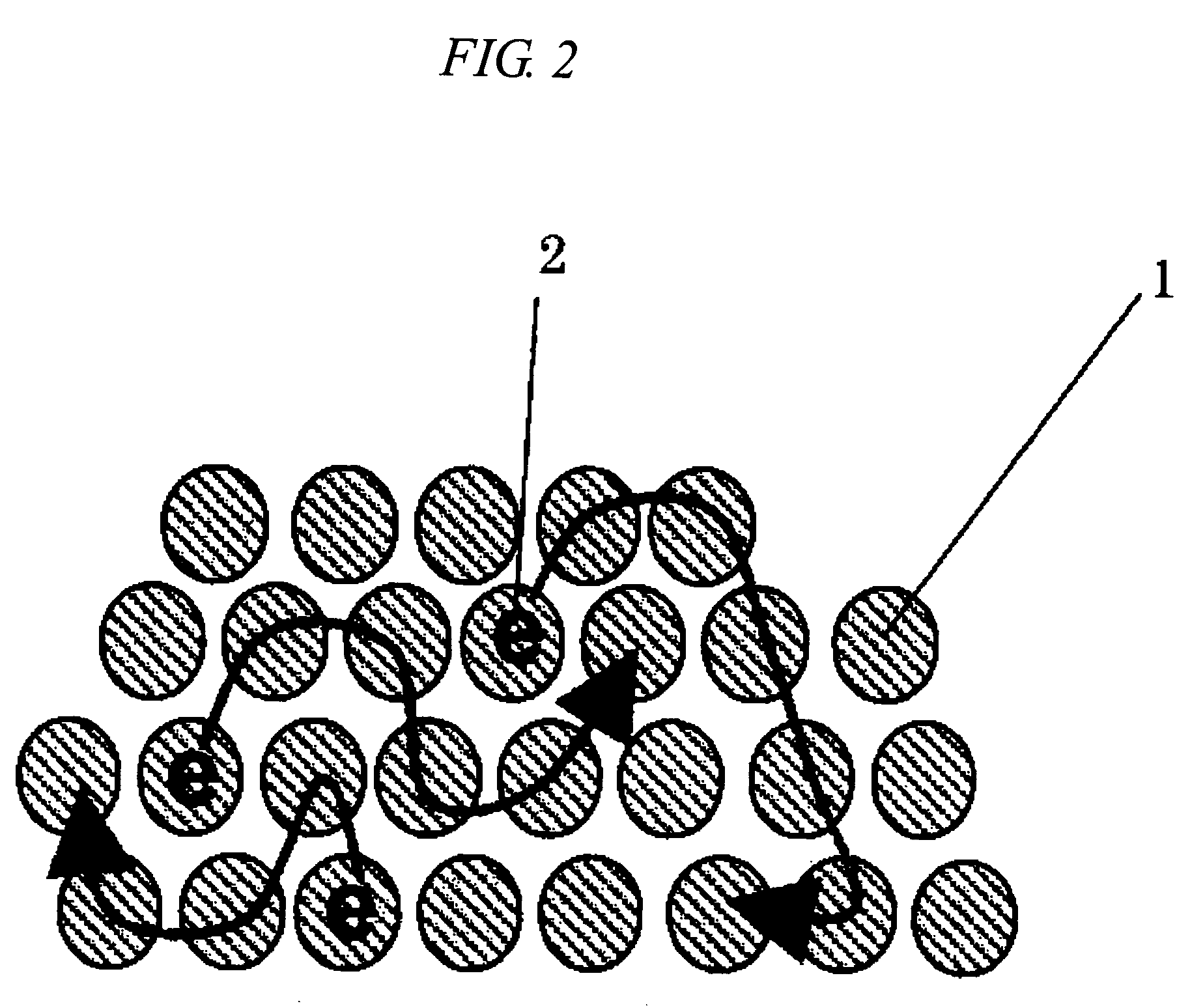
[0052] The method of synthesizing the nanoparticles used for a channel portion of the Mott transistor according to the present invention will be described. First, hydrogen tetrachloroaurate (III) tetrahydrate of 0.31 g is dissolved into the water of 30 ml. Then, toluene of 80 ml is added to the solution and tetra-n-octyl ammonium bromide of 2.2 g is added thereto. Thereafter, the solution is stirred for an hour at a room temperature. Then, 1-dodecanethiol of 170 mg is dropped slowly to the solution, and the solution is stirred for an hour. Meanwhile, sodium borohydride of 0.38 g is dissolved into the water of 25 ml and this is dropped into the above-mentioned solution in 30 minutes, and the resulting solution is stirred for four hours. The solution is separated and an organic layer is concentrated to 10 ml. Then, ethanol of 400 ml is added thereto and the resulting solution is left sitting for 50 hours at −18° C. Thereafter, it is dried under the reduced pressure after removing the ...

second embodiment

[0071] In the above-described first embodiment, since the carriers are not doped into the nanoparticles before applying the gate voltage, the change form metal to insulator is observed when the gate voltage is increased. This second embodiment discloses the method as follows. That is, the doping to the self-organized nanoparticle array is performed in advance so as to achieve the normally off, and then, the Mott transistor is integrated on a flexible substrate.

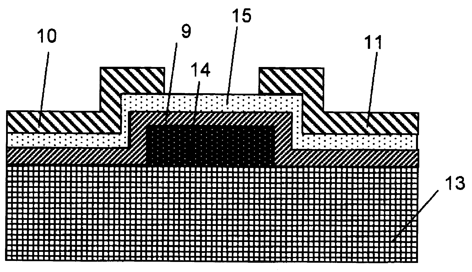
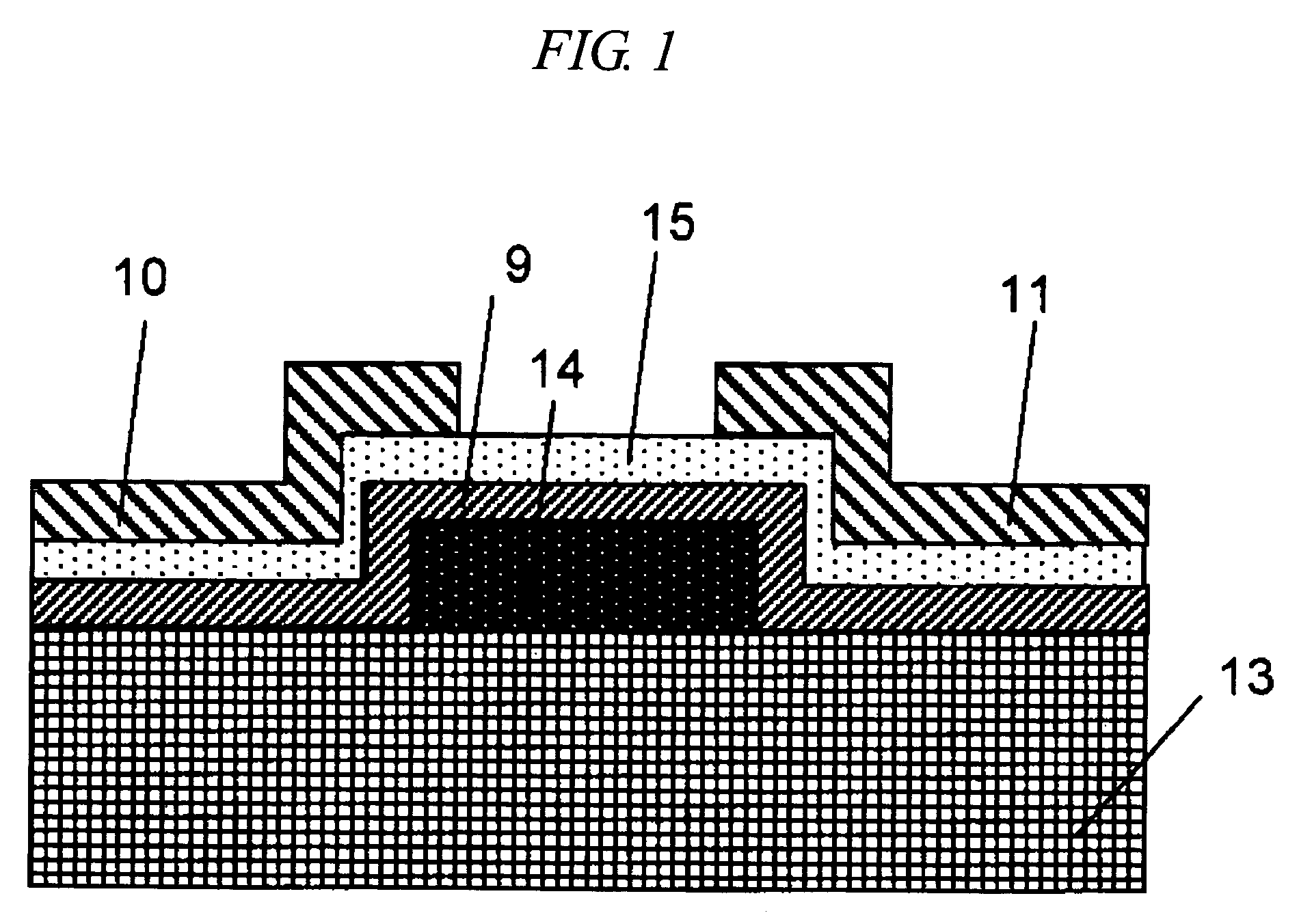
[0072] First, a flexible plastic substrate 13 is prepared and a gold gate electrode 14 is formed thereon by using the lift-off process as shown in FIG. 19. The flexible substrate is made of plastic and is cost effective in comparison to a single crystal silicon substrate. Therefore, it is possible to significantly reduce the cost for manufacturing the device.

[0073] Subsequently, a silicon dioxide gate insulating film 9 with a thickness of about 20 nm is deposited as shown in FIG. 20. Next, the nanoparticles are formed in the...

third embodiment

[0080] This embodiment discloses the method in which an organic semiconductor is bonded to the periphery of the metal nanoparticles so that the effective mobility of the field effect transistor in which the self-aligned nanoparticle array bonded by the organic semiconductor is used for a channel can be increased about ten times.

[0081] At the beginning, the nanoparticles used in this embodiment are formed. First, hydrogen tetrachloroaurate (III) tetrahydrate of 0.37 g is dissolved into the water of 30 ml. Then, chloroform of 80 ml is added to the solution and tetra-n-octyl ammonium bromide of 2.2 g is added thereto. Thereafter, the solution is stirred for an hour at a room temperature. Then, poly(3-hexyl thiophene) of 0.28 g is added to the solution and the resulting solution is stirred for an hour. Further, sodium borohydride of 0.38 g is dissolved into the water of 25 ml and this solution is dropped into the above-described solution in 30 minutes, and the resulting solution is sti...


PUM


Abstract

The Mott transistor capable of operating at a room temperature can be realized by using a self-organized nanoparticle array for the channel portion. The nanoparticle used in the present invention comprises metal and organic molecules, and the size thereof is extremely small, that is, about a few nm. Therefore, the charging energy is sufficiently larger than the thermal energy kBT=26 meV, and the transistor can operate at a room temperature. Also, since the nanoparticles with a diameter of a few nm are arranged in a self-organized manner and the Mott transition can be caused by the change of a number of electrons of the surface density of about 1012 cm−2, the transistor can operate by the gate voltage of about several V.

Description

CROSS-REFERENCE TO RELATED APPLICATION [0001] The present application claims priority from Japanese Patent Application JP 2003-426172 filed on Dec. 24, 2003, the content of which is hereby incorporated by reference into this application. TECHNICAL FIELD OF THE INVENTION [0002] The present invention relates to a field effect transistor and a manufacturing method thereof. More specifically, the present invention relates to a new-type field effect transistor and a manufacturing method thereof, which can simultaneously achieve the low off-current and the high on-current by using the self-organized nanoparticle array as a material of a channel portion and using the metal-insulator transition (Mott transition) as an operational principle thereof. BACKGROUND OF THE INVENTION [0003] The technology for an integrated circuit using silicon has been developing at an amazing pace. With the development of the technology for scaling down, the size of the elements has been reduced and the number of...

Claims


Application Information

Patent Timeline
Patent Type & Authority Applications(United States)
IPC IPC(8): H01L29/78H01L21/335H01L29/76H01L49/00
CPCH01L49/003H01L29/7613H10N99/03C09K11/06H01L29/783H01L29/7833H01L29/78618H01L29/78645H01L29/78696H01L2924/1307
Inventor SAITO, SHIN-ICHIARAI, TADASHIHISAMOTO, DIGHTSUCHIYA, RYUTAFUKUDA, HIROSHIONAI, TAKAHIRO
Owner HITACHI LTD
Why Eureka
Try Eureka