Electromagnetic wave absorber, method of manufacturing the same and appliance using the same

a technology of electromagnetic waves and absorbers, applied in the field of electromagnetic waves absorbers, can solve the problems of erroneous equipment operation, unfavorable noise emission, deterioration of noise environment inside equipment, etc., and achieve the effect of suppressing noise inside the module, good and excellent electromagnetic wave absorption characteristi

Inactive Publication Date: 2005-06-30
HITACHI LTD
View PDF24 Cites 16 Cited by
  • Summary
  • Abstract
  • Description
  • Claims
  • Application Information

AI Technical Summary

Benefits of technology

[0058] In accordance with the present invention, in an optical sending or receiving module comprising an electric-optical converter used for a high speed communication network, by covering an optical sending element or an optical receiving element and the related circuit with an electromagnetic wave absorber having composite magnetic particles and the ceramic, or with an electromagnetic wave absorber in which the composite magnetic particles and a material having an electric resistivity higher than that of the composite magnetic particle are unified, the electromagnetic wave emitted outside the module and the noise interference inside the module can be suppressed. The electromagnetic wave absorber used in accordance with the present invention is the same as described above.
[0059] According to the present invention, the electromagnetic wave absorber composed of the composite magnetic particles in which the magnetic metal and the non-magnetic or magnetic ceramics are unified in ultra-finely dispersed manner can obtain the remarkable effect of having an excellent electromagnetic wave absorption characteristic compared to the electromagnetic wave absorber made of the simply mixed powder.
[0060] Further, according to the present invention, the electromagnetic wave absorber is formed by unifying the composite magnetic particles, each of which is composed of fine crystal grains of the magnetic metal (the magnetic metal grains) and the ceramic phase, particularly, fine crystal grains including at least one kind of non-magnetic or magnetic oxide, carbide and nitride, and the material having an electric resistivity higher than that of the composite magnetic particles. The electromagnetic wave absorber has a good electromagnetic wave absorption characteristic in the high frequency region, particularly, in the GHz region, and can be formed as a thin electromagnetic wave absorber, and can efficiently suppress electromagnetic wave interference inside the electronic equipment.

Problems solved by technology

In recent years, there have been significant advances in high speed processing in electronic equipment, and the operating frequency of an IC, such as an LSI or a microprocessor, has rapidly increased, with the result that undesirable noises are likely to be emitted.
Thus, in recent electronic equipment, due to a decrease in the noise margin due to a reduction in the electric power consumed by the equipment and by a decrease in the immunity (noise resistance) due to replacement of digital circuits to analogue circuits and the tendency of small-sizing and high-mounting density, the noise environment inside the equipment has been deteriorated, thereby to cause a problem of erroneous operation of the equipment due to electromagnetic interference (hereinafter, referred to as EMI).
Further, in regard to the complex specific dielectric constant, since the imaginary part is large compared to the real part, because the electric resistivity is not sufficiently high, it is difficult to adjust the impedance matching.
However, no electromagnetic wave absorber capable of satisfying all of these characteristics has been developed as yet.
However, as the value of the complex specific magnetic permeability becomes large, it is difficult to adjust the impedance matching of the substance with the free space.
However, in the high frequency region, the specific magnetic permeability is substantially decreased and the imaginary part of the complex specific dielectric constant is substantially increased due to eddy current loss because the electric resistivity is low.
Therefore, the reflection becomes large, and the soft magnetic metallic material does not work as an electromagnetic wave absorber.
However, the electromagnetic wave absorber has problems in that the cost is high because a large film-forming apparatus is required, and the use of the electromagnetic wave absorber is limited because of the thin-film structure.
However, it does not have a sufficient thickness and absorption ability as an electromagnetic wave absorber used inside of electronic equipment or used for a high frequency region.
However, this publication does not propose to use the magnetic thin films as an electromagnetic wave absorber.
However, the publication does not propose any electromagnetic wave absorber.

Method used


Image

  • Electromagnetic wave absorber, method of manufacturing the same and appliance using the same
  • Electromagnetic wave absorber, method of manufacturing the same and appliance using the same
  • Electromagnetic wave absorber, method of manufacturing the same and appliance using the same

Examples


embodiment 1

[0081] A mixed powder consisting of Fe powder of 50 vol % having grain size of 1 to 5 μm and SiO2 powder of 50 vol % having an average grain size of 0.3 μm, and balls made of SUS410 (diameter: 9.5 mm) with a weight ratio of the powders to the balls=1 to 80 were put into a pot made of stainless steel, and the pot was filled with argon gas, and MA (mechanical alloying) treatment was performed thereon at a rotation speed of 200 rpm for 100 hours. The composite magnetic particles after the MA was of indefinite shape, having complicated shapes, and the average particle size was several tens μm.

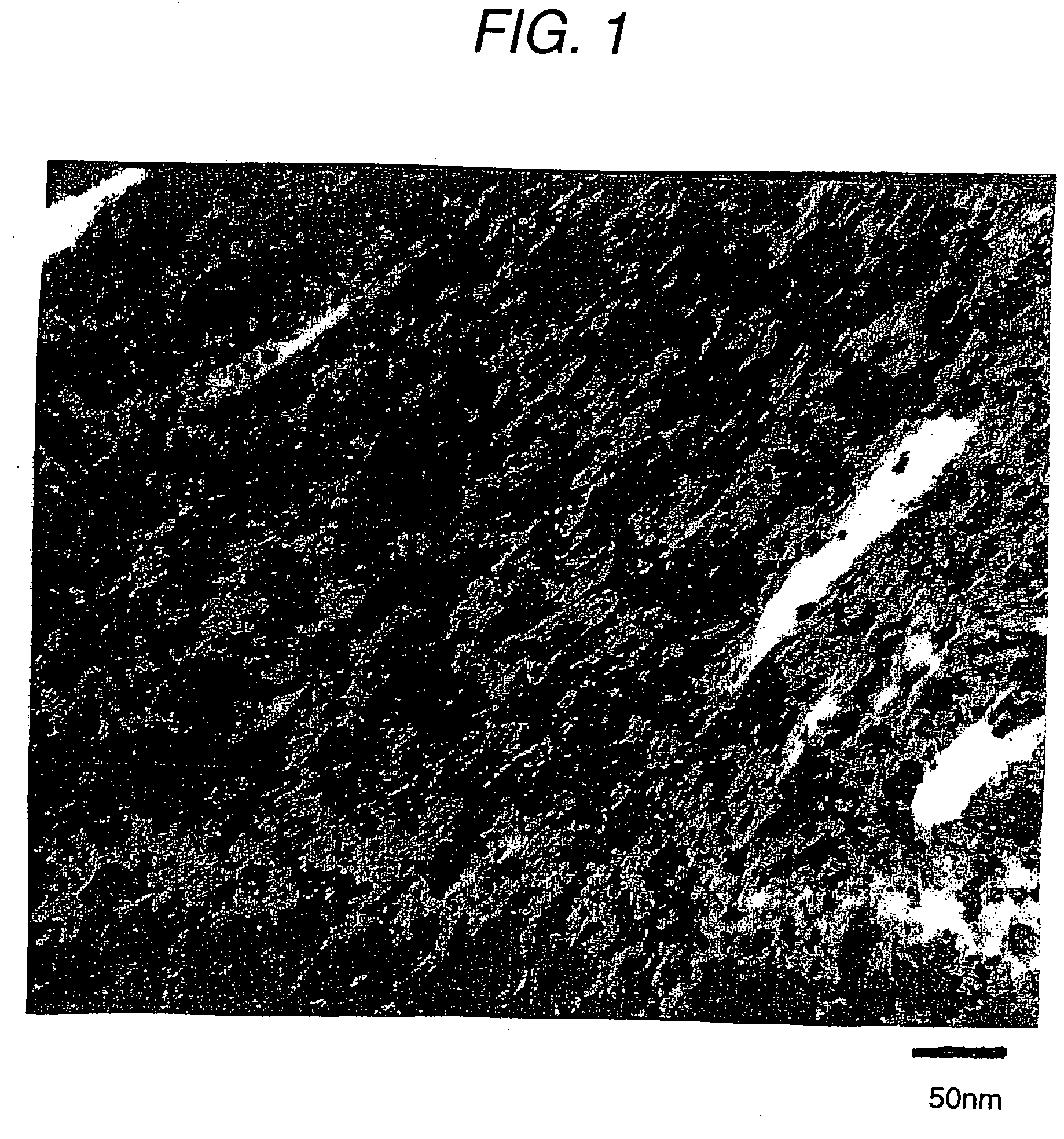
[0082]FIG. 1 is a photograph of the structure obtained from observation of the composite magnetic particle using a TEM. The crystal grain size of Fe of the black portion in the photograph is 10 nm, and the composite magnetic particle has a complicated shape, and Si oxide of the white portion is formed in a network-shape so as to enclose Fe grains having a grain size below 100 nm. The fine Fe grain...

embodiment 2

[0091] A mixed powder consisting of Fe powder having a grain size of 1 to 5 μm and soft magnetic metal oxide powder of (Ni—Zn—Cu)Fe2O4 or (Mn—Zn)Fe2O4 (50:50 in volume ratio) having an average grain size of 0.7 μm, and balls made of SUS410 (diameter: 9.5 mm) with a weight ratio of the powders to the balls=1 to 80 were put into a pot made of stainless steel, and the pot was filled with argon gas, and MA (mechanical alloying) treatment was performed at a rotation speed of 200 rpm for 100 hours. The composite magnetic particles after the MA was of indefinite shape, and the average particle size was several tens μm. Further, the result of observing the composite magnetic particle using a TEM was similar to that of Embodiment 1. The crystal grain size of Fe was about 10 nm, and oxides including components of the soft magnetic metal oxide were finely dispersed in a network shape in the crystal grain boundary. Annealing of the composite magnetic particles was performed in a vacuum (the deg...

embodiment 3

[0093] A powder obtained by mixing Fe powder having a grain size of 1 to 5 μm and Si powder having an average grain size of 1.0 μm of 50:50 in volume ratio, and the same balls made of SUS410 as described above with a weight ratio of the powders to the balls=1 to 80 were put into a pot made of stainless steel together, and the pot was filled with oxygen gas (Ar:O2=4:1), and mechanical alloying (MA) treatment was performed at a rotation speed of 200 rpm for 100 hours. The composite powder after the MA was of indefinite shape, and the average particle size was 5.0 μm. Further, as a result of observing the composite magnetic particle using a TEM, the crystal grain size of Fe was about 10 nm, and oxides including components of Si oxide were finely dispersed in a network shape in the crystal grain boundary. Further, as a result of an X-ray diffraction analysis, it was checked that there were Fe oxides (Fe2O3, Fe3O4). Similarly to the method described above, various kinds of characteristic...


PUM

PropertyMeasurementUnit
grain sizeaaaaaaaaaa
electric resistivityaaaaaaaaaa
grain sizeaaaaaaaaaa

Abstract

An electromagnetic wave absorber for use in the high frequency range above 1 Ghz and a composite member are characterized by the fact that magnetic metal grains are covered with ceramic above 20 volume %. Further, a method of manufacturing the electromagnetic absorber and the composite member is characterized by the fact that composite magnetic particles, in which a plurality of magnetic metal grains and ceramic are unified, are formed through a mechanical alloying method applied to a composite powder composed of magnetic metal powder and ceramic powder. The electromagnetic wave absorber can be used in a semiconductor device, an optical sending module, an optical receiving module, an optical sending and receiving module, an automatic tollgate in which erroneous operation due to electromagnetic wave disturbance is provided by use of the electromagnetic wave absorber.

Description

BACKGROUND OF THE INVENTION [0001] The present invention relates to a novel electromagnetic wave absorber, a method of manufacturing the electromagnetic wave absorber, a composite member and an appliance of the electromagnetic wave absorber. More particularly, the invention relates to an electromagnetic wave absorber comprising composite magnetic particles composed of magnetic metal grains and ceramics, particularly, fine crystalline grains containing at least one kind of material selected from the group consisting of non-magnetic or soft magnetic metal oxides, carbides and nitrides. The invention also relates to a method of manufacturing the electromagnetic wave absorber, a composite member using the electromagnetic wave absorber, and a semiconductor device, a printed wire board, an optical sending and receiving module, an electronic toll collection system and an electronic device casing using the magnetic metal particles. [0002] In accordance with the present invention, an optical...

Claims


Application Information

Patent Timeline
Patent Type & Authority Applications(United States)
IPC IPC(8): H01F1/04H01L23/552H01Q17/00H05K1/02H05K9/00
CPCH01L23/552Y10T428/252H01L2224/32145H01L2224/48095H01L2224/48227H01L2924/01012H01L2924/01025H01L2924/01046H01L2924/01079H01L2924/15311H01L2924/16152H01L2924/19041H01L2924/3011H01L2924/3025H01Q17/001H01Q17/004H05K1/0233H05K9/0083H01L24/48H01L2224/45124H01L2224/16Y10T428/2982Y10T428/2993Y10T428/25H01L2224/32225H01L2224/16225H01L2224/73265H01L2924/00H01L2224/45144H01L2224/45147H01L2924/00014H01L2924/12042H01L24/45H01L2924/14H01L2924/181H01L2224/05599H01L2924/00012H01F1/04
Inventor FUJIEDA, TADASHIIKEDA, SHINZOUOGAWA, SAIABE, TERUYOSHIAONO, YASUHISA
Owner HITACHI LTD
Why Eureka
Try Eureka